
Videos
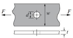
The maximum stress smax at the edge of a hole (diameter d) in a thin plate. F with width w and thickness t, loaded by a tensile force F as shown is given by:
Write a program in a script file that calculates smax. The program should read the values of F, w, d, and t from an ASCII text file using the load command. The output should be in the form of a paragraph combining text and numbers i.e., something like: “The maximum stress in a plate with a width of XX in. and thickness of XX in. and a hole of XX in. in diameter, due to a tensile force of XXX lb is XXXX psi, where XX stands for numerical values.” The stress should be rounded to the nearest integer. Use the program to calculate smaxwhen w=2.5in., d=1.375in., t=0.1875 in., and F=8000 lb.
Want to see the full answer?
Check out a sample textbook solution
Chapter 4 Solutions
EBK MATLAB: AN INTRODUCTION WITH APPLIC


- I have uploaded the rules, please explain step by step and which rule you have appliedarrow_forwardUsing the CCS Compiler method to solve this question Write a PIC16F877A program that flash ON the 8-LED's connected to port-B by using two switches connected to port-D (Do & D₁) as shown in figure below, according to the following scenarios: (Hint: Use 500ms delay for each case with 4MHz frequency) 1. When Do=1 then B₁,B3,B7 are ON. 2. When Do 0 then Bo,B2, B4, B5, B6 are ON. 3. When D₁=1 then B4,B,,B6,B7 are ON. 4. When D₁-0 then Bo,B1,B2,B3 are ON.arrow_forwardUse the ramp generator circuit in Fig. B2a to generate the waveform shown in Fig. B2b. Write four equations relating resistors R1, R2, R3, capacitor C and voltages Vs, VR and VA.to the waveform parameters T₁, T, Vcm and Vm- If R = R2 = R3, R₁ = 2R, C = 1 nF, Vcm = 2 V and Vm = 1 V, T₁ = 2 μs and T = 10 μs solve for the values of R, Vs, VR and VA using your equations from part a(i). VR C +VA R3 V₂ Vo мат R1 VsO+ V₁ R₂ Figure B2a Vout Vcm+Vm Vcm Vcm-Vm 0 T₁ T 2T time Figure B2barrow_forward
- The circuit in Figure B1a is a common analogue circuit block. Explain why you would need such a circuit. Draw another circuit in which you use the current flowing in this loop to bias a common source amplifier. This circuit is not ideal for standard CMOS technologies due to threshold shift. Why? Draw an improved version of this circuit to make it better. VDD (W)P MA M3. (), REF (쁜)~ M₁ M2 lout 시~ Rsarrow_forward23bcarrow_forwardDraw the small-signal equivalent circuit of a single transistor amplifier given in figure B1b. Assume the current source to be ideal. Determine the Open-loop transfer function, pole frequency and gain-bandwidth product all in terms of transistor parameters 9m, To and CL. If the load capacitance is 1pF and the necessary unity gain frequency is 600MHz, find the gm for this transistor. V₁ V₁ CLarrow_forward
 Introductory Circuit Analysis (13th Edition)Electrical EngineeringISBN:9780133923605Author:Robert L. BoylestadPublisher:PEARSON
 Delmar's Standard Textbook Of ElectricityElectrical EngineeringISBN:9781337900348Author:Stephen L. HermanPublisher:Cengage Learning
 Programmable Logic ControllersElectrical EngineeringISBN:9780073373843Author:Frank D. PetruzellaPublisher:McGraw-Hill Education
 Fundamentals of Electric CircuitsElectrical EngineeringISBN:9780078028229Author:Charles K Alexander, Matthew SadikuPublisher:McGraw-Hill Education
 Electric Circuits. (11th Edition)Electrical EngineeringISBN:9780134746968Author:James W. Nilsson, Susan RiedelPublisher:PEARSON
 Engineering ElectromagneticsElectrical EngineeringISBN:9780078028151Author:Hayt, William H. (william Hart), Jr, BUCK, John A.Publisher:Mcgraw-hill Education,