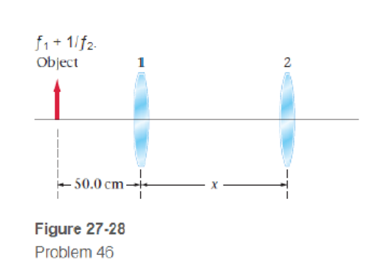
Two lenses, with f 1 = +20.0 cm and f 2 = +30.0 cm, are placed on the x axis, as shown in Figure 27-28 An object is fixed 50 0 cm to the left of lens 1, and lens 2 is a variable distance x to the right of lens 1. Find the lateral magnification and location of the final image relative to lens 2 for the following cases: (a) x = 115 cm; (b) x = 30.0 cm; (c) x = 0 (d) Show that your result for part (c) agrees with the relation for the effective focal length of two lenses in contact, 1/ f eff = 1.
Two lenses, with f 1 = +20.0 cm and f 2 = +30.0 cm, are placed on the x axis, as shown in Figure 27-28 An object is fixed 50 0 cm to the left of lens 1, and lens 2 is a variable distance x to the right of lens 1. Find the lateral magnification and location of the final image relative to lens 2 for the following cases: (a) x = 115 cm; (b) x = 30.0 cm; (c) x = 0 (d) Show that your result for part (c) agrees with the relation for the effective focal length of two lenses in contact, 1/ f eff = 1.
Two lenses, with f1 = +20.0 cm and f2 = +30.0 cm, are placed on the x axis, as shown in Figure 27-28 An object is fixed 50 0 cm to the left of lens 1, and lens 2 is a variable distance x to the right of lens 1. Find the lateral magnification and location of the final image relative to lens 2 for the following cases: (a)x = 115 cm; (b)x = 30.0 cm; (c)x = 0 (d) Show that your result for part (c) agrees with the relation for the effective focal length of two lenses in contact, 1/feff = 1.
How can you tell which vowel is being produced here ( “ee,” “ah,” or “oo”)? Also, how would you be able to tell for the other vowels?
You want to fabricate a soft microfluidic chip like the one below. How would you go about
fabricating this chip knowing that you are targeting a channel with a square cross-sectional
profile of 200 μm by 200 μm. What materials and steps would you use and why? Disregard the
process to form the inlet and outlet.
Square Cross Section
1. What are the key steps involved in the fabrication of a semiconductor device.
2. You are hired by a chip manufacturing company, and you are asked to prepare a silicon wafer
with the pattern below. Describe the process you would use.
High Aspect
Ratio
Trenches
Undoped Si Wafer
P-doped Si
3. You would like to deposit material within a high aspect ratio trench. What approach would you
use and why?
4. A person is setting up a small clean room space to carry out an outreach activity to educate high
school students about patterning using photolithography. They obtained a positive photoresist, a
used spin coater, a high energy light lamp for exposure and ordered a plastic transparency mask
with a pattern on it to reduce cost. Upon trying this set up multiple times they find that the full
resist gets developed, and they are unable to transfer the pattern onto the resist. Help them
troubleshoot and find out why pattern of transfer has not been successful.
5. You are given a composite…
Need a deep-dive on the concept behind this application? Look no further. Learn more about this topic, physics and related others by exploring similar questions and additional content below.


 Principles of Physics: A Calculus-Based TextPhysicsISBN:9781133104261Author:Raymond A. Serway, John W. JewettPublisher:Cengage Learning
 University Physics Volume 3PhysicsISBN:9781938168185Author:William Moebs, Jeff SannyPublisher:OpenStax
 Physics for Scientists and Engineers, Technology ...PhysicsISBN:9781305116399Author:Raymond A. Serway, John W. JewettPublisher:Cengage Learning
 College PhysicsPhysicsISBN:9781285737027Author:Raymond A. Serway, Chris VuillePublisher:Cengage Learning
 Physics for Scientists and EngineersPhysicsISBN:9781337553278Author:Raymond A. Serway, John W. JewettPublisher:Cengage Learning
 Physics for Scientists and Engineers with Modern ...PhysicsISBN:9781337553292Author:Raymond A. Serway, John W. JewettPublisher:Cengage Learning