Predict/Calculate When a charged particle enters a region of uniform magnetic field, it follows a circular path, as indicated in Figure 22-44 . (a) Is this particle positively or negatively charged? Explain. (b) Suppose that the magnetic field has a magnitude of 0.180 T, the particle’s speed is 6.0 × 10 6 m/s, and the radius of its path is 52.0 cm. Find the mass of the particle, given that its charge has a magnitude of 1.60 × 10 −19 C. Give your result in atomic mass units, u, where 1 u = 1.67 × 10 −27 kg. Figure 22-44 Problem 23
Predict/Calculate When a charged particle enters a region of uniform magnetic field, it follows a circular path, as indicated in Figure 22-44 . (a) Is this particle positively or negatively charged? Explain. (b) Suppose that the magnetic field has a magnitude of 0.180 T, the particle’s speed is 6.0 × 10 6 m/s, and the radius of its path is 52.0 cm. Find the mass of the particle, given that its charge has a magnitude of 1.60 × 10 −19 C. Give your result in atomic mass units, u, where 1 u = 1.67 × 10 −27 kg. Figure 22-44 Problem 23
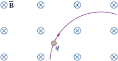
Predict/Calculate When a charged particle enters a region of uniform magnetic field, it follows a circular path, as indicated in Figure 22-44. (a) Is this particle positively or negatively charged? Explain. (b) Suppose that the magnetic field has a magnitude of 0.180 T, the particle’s speed is 6.0 × 10⁶ m/s, and the radius of its path is 52.0 cm. Find the mass of the particle, given that its charge has a magnitude of 1.60 × 10⁻¹⁹ C. Give your result in atomic mass units, u, where 1 u = 1.67 × 10⁻²⁷ kg.
You want to fabricate a soft microfluidic chip like the one below. How would you go about
fabricating this chip knowing that you are targeting a channel with a square cross-sectional
profile of 200 μm by 200 μm. What materials and steps would you use and why? Disregard the
process to form the inlet and outlet.
Square Cross Section
1. What are the key steps involved in the fabrication of a semiconductor device.
2. You are hired by a chip manufacturing company, and you are asked to prepare a silicon wafer
with the pattern below. Describe the process you would use.
High Aspect
Ratio
Trenches
Undoped Si Wafer
P-doped Si
3. You would like to deposit material within a high aspect ratio trench. What approach would you
use and why?
4. A person is setting up a small clean room space to carry out an outreach activity to educate high
school students about patterning using photolithography. They obtained a positive photoresist, a
used spin coater, a high energy light lamp for exposure and ordered a plastic transparency mask
with a pattern on it to reduce cost. Upon trying this set up multiple times they find that the full
resist gets developed, and they are unable to transfer the pattern onto the resist. Help them
troubleshoot and find out why pattern of transfer has not been successful.
5. You are given a composite…
Two complex values are z1=8 + 8i, z2=15 + 7 i. z1∗ and z2∗ are the complex conjugate values.
Any complex value can be expessed in the form of a+bi=reiθ. Find r and θ for (z1-z∗2)/z1+z2∗. Find r and θ for (z1−z2∗)z1z2∗ Please show all steps
Need a deep-dive on the concept behind this application? Look no further. Learn more about this topic, physics and related others by exploring similar questions and additional content below.


 College PhysicsPhysicsISBN:9781938168000Author:Paul Peter Urone, Roger HinrichsPublisher:OpenStax College
 Principles of Physics: A Calculus-Based TextPhysicsISBN:9781133104261Author:Raymond A. Serway, John W. JewettPublisher:Cengage Learning
 Physics for Scientists and Engineers with Modern ...PhysicsISBN:9781337553292Author:Raymond A. Serway, John W. JewettPublisher:Cengage Learning
 College PhysicsPhysicsISBN:9781305952300Author:Raymond A. Serway, Chris VuillePublisher:Cengage Learning
 College PhysicsPhysicsISBN:9781285737027Author:Raymond A. Serway, Chris VuillePublisher:Cengage Learning
 Physics for Scientists and Engineers: Foundations...PhysicsISBN:9781133939146Author:Katz, Debora M.Publisher:Cengage Learning