
Videos
(a)
Design a circuit which produces a transfer function of
(a)
Explanation of Solution
Problem design:
Synthesize a circuit that will yield the transfer function
Calculation:
The transfer function of the circuit is,
The above equation is written as,
For the above transfer function, it has two repeated zeros at
The Figure 14.39 (b) in the textbook, that shows a cascade two stages of the circuit with a zero at
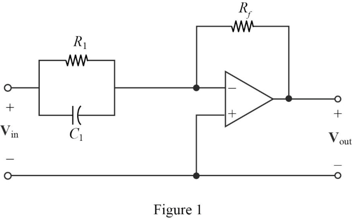
For a single zero,
Substitute
Let arbitrarily consider
Substitute
Transfer function:
The input impedance of the cascaded circuit is,
Then, write the Formula for the transfer function for the cascaded two stage amplifier.
Substitute
Thus, consider that the transfer function for
Substitute 1 for
Completing the design by letting
Since, two repeated zeros at
Therefore,
Substitute
Thus, the final design of the circuit is,
Conclusion:
Thus, a circuit is designed which produces a transfer function of
(b)
Design a circuit which produces a transfer function of
(b)
Explanation of Solution
Problem design:
Synthesize a circuit that will yield the transfer function
Calculation:
The transfer function of the circuit is,
Consider the transfer function for the cascaded circuit as below.
The above transfer function, it has two poles at
The Figure 14.39 (a) in the textbook, that shows a cascade two stages of the circuit with pole at
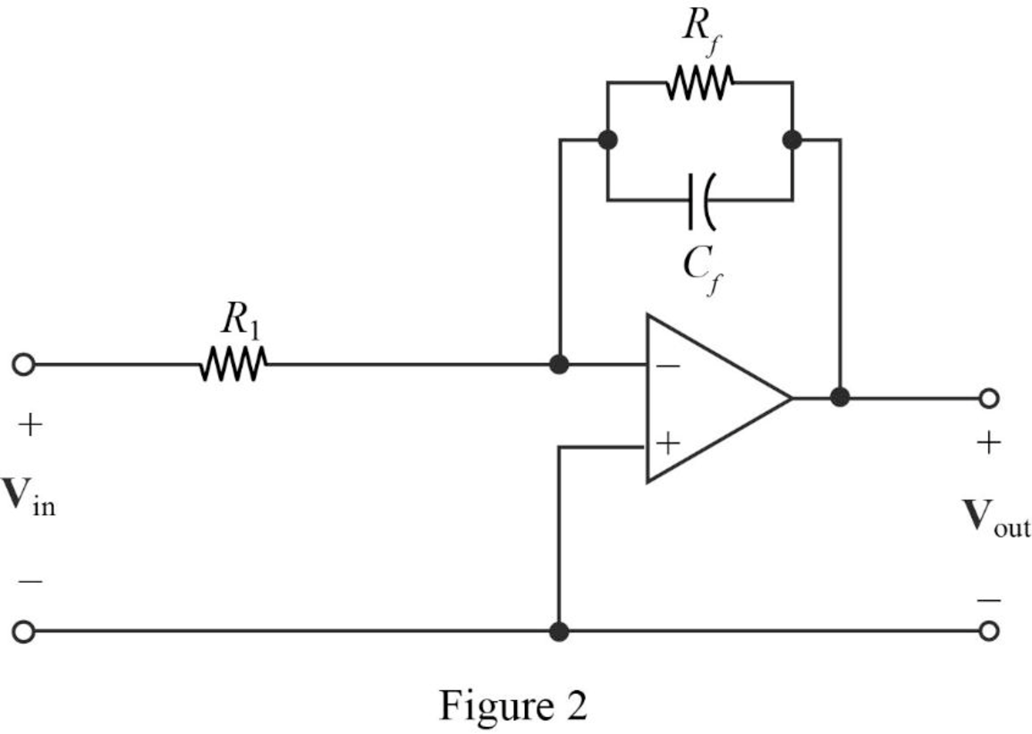
The above Figure 2, is the representation for the first stage and second stage of a cascaded circuit to be drawn.
Consider the denominator of given transfer function and the first pole as
Where,
Substitute
Let arbitrarily consider
Substitute
Transfer function:
Find the feedback impedance of the cascaded circuit in Figure 2.
Write the formula for the transfer function of the cascaded circuit in Figure 2 as follows
Substitute
Therefore, consider the transfer function for the first pole
Substitute 500 for
Completing the design by letting
Consider the denominator of given transfer function and the first pole as
Where,
Substitute
Arbitrarily consider
Substitute
Therefore, consider the transfer function for the second pole
Substitute 100 for
Completing the design by letting
Then, from the transfer function of the two stages write the complete transfer function as follows.
Substitute
Thus, the final design of the circuit is,
Conclusion:
Thus, a circuit is designed which produces a transfer function of
Want to see more full solutions like this?
Chapter 14 Solutions
Engineering Circuit Analysis


- 2. Using the approximate method, hand sketch the Bode plot for the following transfer functions. a) H(s) = 10 b) H(s) (s+1) c) H(s): = 1 = +1 100 1000 (s+1) 10(s+1) d) H(s) = (s+100) (180+1)arrow_forwardQ4: Write VHDL code to implement the finite-state machine described by the state Diagram in Fig. 1. Fig. 1arrow_forward1. Consider the following feedback system. Bode plot of G(s) is shown below. Phase (deg) Magnitude (dB) -50 -100 -150 -200 0 -90 -180 -270 101 System: sys Frequency (rad/s): 0.117 Magnitude (dB): -74 10° K G(s) Bode Diagram System: sys Frequency (rad/s): 36.8 Magnitude (dB): -99.7 System: sys Frequency (rad/s): 20 Magnitude (dB): -89.9 System: sys Frequency (rad/s): 20 Phase (deg): -143 System: sys Frequency (rad/s): 36.8 Phase (deg): -180 101 Frequency (rad/s) a) Determine the range of K for which the closed-loop system is stable. 102 10³ b) If we want the gain margin to be exactly 50 dB, what is value for K we should choose? c) If we want the phase margin to be exactly 37°, what is value of K we should choose? What will be the corresponding rise time (T) for step-input? d) If we want steady-state error of step input to be 0.6, what is value of K we should choose?arrow_forward
- : Write VHDL code to implement the finite-state machine/described by the state Diagram in Fig. 4. X=1 X=0 solo X=1 X=0 $1/1 X=0 X=1 X=1 52/2 $3/3 X=1 Fig. 4 X=1 X=1 56/6 $5/5 X=1 54/4 X=0 X-O X=O 5=0 57/7arrow_forwardQuestions: Q1: Verify that the average power generated equals the average power absorbed using the simulated values in Table 7-2. Q2: Verify that the reactive power generated equals the reactive power absorbed using the simulated values in Table 7-2. Q3: Why it is important to correct the power factor of a load? Q4: Find the ideal value of the capacitor theoretically that will result in unity power factor. Vs pp (V) VRIPP (V) VRLC PP (V) AT (μs) T (us) 8° pf Simulated 14 8.523 7.84 84.850 1000 29.88 0.866 Measured 14 8.523 7.854 82.94 1000 29.85 0.86733 Table 7-2 Power Calculations Pvs (mW) Qvs (mVAR) PRI (MW) Pay (mW) Qt (mVAR) Qc (mYAR) Simulated -12.93 -7.428 9.081 3.855 12.27 -4.84 Calculated -12.936 -7.434 9.083 3.856 12.32 -4.85 Part II: Power Factor Correction Table 7-3 Power Factor Correction AT (us) 0° pf Simulated 0 0 1 Measured 0 0 1arrow_forwardQuestions: Q1: Verify that the average power generated equals the average power absorbed using the simulated values in Table 7-2. Q2: Verify that the reactive power generated equals the reactive power absorbed using the simulated values in Table 7-2. Q3: Why it is important to correct the power factor of a load? Q4: Find the ideal value of the capacitor theoretically that will result in unity power factor. Vs pp (V) VRIPP (V) VRLC PP (V) AT (μs) T (us) 8° pf Simulated 14 8.523 7.84 84.850 1000 29.88 0.866 Measured 14 8.523 7.854 82.94 1000 29.85 0.86733 Table 7-2 Power Calculations Pvs (mW) Qvs (mVAR) PRI (MW) Pay (mW) Qt (mVAR) Qc (mYAR) Simulated -12.93 -7.428 9.081 3.855 12.27 -4.84 Calculated -12.936 -7.434 9.083 3.856 12.32 -4.85 Part II: Power Factor Correction Table 7-3 Power Factor Correction AT (us) 0° pf Simulated 0 0 1 Measured 0 0 1arrow_forward
- electric plants. Prepare the load schedulearrow_forwardelectric plants Draw the column diagram. Calculate the voltage drop. by hand writingarrow_forwardelectric plants. Draw the lighting, socket, telephone, TV, and doorbell installations on the given single-story project with an architectural plan by hand writingarrow_forward
- A circularly polarized wave, traveling in the +z-direction, is received by an elliptically polarized antenna whose reception characteristics near the main lobe are given approx- imately by E„ = [2â, + jâ‚]ƒ(r. 8, 4) Find the polarization loss factor PLF (dimensionless and in dB) when the incident wave is (a) right-hand (CW) An elliptically polarized wave traveling in the negative z-direction is received by a circularly polarized antenna. The vector describing the polarization of the incident wave is given by Ei= 2ax + jay.Find the polarization loss factor PLF (dimensionless and in dB) when the wave that would be transmitted by the antenna is (a) right-hand CParrow_forwardjX(1)=j0.2p.u. jXa(2)=j0.15p.u. jxa(0)=0.15 p.u. V₁=1/0°p.u. V₂=1/0° p.u. 1 jXr(1) = j0.15 p.11. jXT(2) = j0.15 p.u. jXr(0) = j0.15 p.u. V3=1/0° p.u. А V4=1/0° p.u. 2 jX1(1)=j0.12 p.u. 3 jX2(1)=j0.15 p.u. 4 jX1(2)=0.12 p.11. JX1(0)=0.3 p.u. jX/2(2)=j0.15 p.11. X2(0)=/0.25 p.1. Figure 1. Circuit for Q3 b).arrow_forwardcan you show me full workings for this problem. the solution is - v0 = 10i2 = 2.941 volts, i0 = i1 – i2 = (5/3)i2 = 490.2mA.arrow_forward
 Introductory Circuit Analysis (13th Edition)Electrical EngineeringISBN:9780133923605Author:Robert L. BoylestadPublisher:PEARSON
 Delmar's Standard Textbook Of ElectricityElectrical EngineeringISBN:9781337900348Author:Stephen L. HermanPublisher:Cengage Learning
 Programmable Logic ControllersElectrical EngineeringISBN:9780073373843Author:Frank D. PetruzellaPublisher:McGraw-Hill Education
 Fundamentals of Electric CircuitsElectrical EngineeringISBN:9780078028229Author:Charles K Alexander, Matthew SadikuPublisher:McGraw-Hill Education
 Electric Circuits. (11th Edition)Electrical EngineeringISBN:9780134746968Author:James W. Nilsson, Susan RiedelPublisher:PEARSON
 Engineering ElectromagneticsElectrical EngineeringISBN:9780078028151Author:Hayt, William H. (william Hart), Jr, BUCK, John A.Publisher:Mcgraw-hill Education,