The

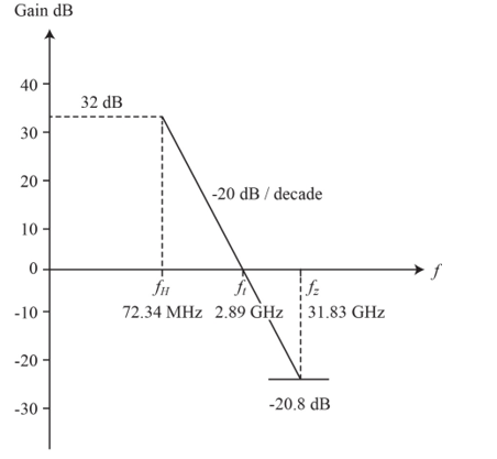
Fig: Bode plot
Given Information:
Calculation:
The expression for gain in the CS amplifier is given by,
Where
Plugging given values.
Write the equation for 3-dB frequency in terms of capacitance
Plugging given values.
The equation for unity gain frequency in terms of trans-conductance
The equation for the frequency of the transmission zero in terms of trans-conductance
Plugging value for parameters


Fig: Bode plot
Want to see the full answer?
Check out a sample textbook solution
Chapter 10 Solutions
Microelectronic Circuits (the Oxford Series In Electrical And Computer Engineering)
- Solve the following nonlinear system using Newton's method 1 f1(x1, x2, x3)=3x₁ = cos(x2x3) - - 2 f2(x1, x2, x3) = x² - 81(x2 +0.1)² + sin x3 + 1.06 f3(x1, x2, x3) = ex1x2 +20x3 + Using x (0) X1 X2 X3 10π-3 3 = 0.1, 0.1, 0.1 as initial conditioarrow_forwardUse Newton-Raphson method to solve the system x² - 2x-y+0.5= 0 x² + 4y² 4 = 0 - with the starting value (xo,yo) = (2,0.25) and two iteration number.arrow_forwardReversing 3⍉ Motors using manual starters with wiring diagram of forward contacts and reverse contacts.arrow_forward
- Determine (a) the input impedance and (b) the reflectedimpedance, both at terminals (a,b) in the circuit of Fig. P11.14.arrow_forward11.4 Determine Vout in the circuit shown in Fig. P11.4.arrow_forwardFor the circuit in Fig. P11.1, determine (a) iL(t) and (b) theaverage power dissipated in RL.arrow_forward
- Design a synchronous Up/Down counter to produce the following sequence (4 9 2,0,7,6,3,1,5) using T flip-flop. The counter should count up when Up/Down =1, and down when Up/Down = 0.arrow_forwardSolve the following systems using Gauss Seidal and Jacobi iteration methods for n=8 and initial values X0=(000). - 2x16x2 x3 = -38 - -3x1 x2+7x3 = −34 -8x1 + x2 - 2x3 = -20arrow_forwardSolve the following systems using Gauss Seidal and Jacobi iteration methods for n=8 and initial values Xº=(000). 3x12x2x3 = 4 - 2x1 x2 + 2x3 = 10 x13x24x3 = 4arrow_forward
- Use Newton-Raphson method to solve the system x² - 2x-y+0.5= 0 x² + 4y² 4 = 0 - with the starting value (xo,yo) = (2,0.25) and two iteration number.arrow_forwardSolve the following systems using Gauss Seidal and Jacobi iteration methods for n=8 and initial values X0=(000). - 2x16x2 x3 = -38 - -3x1 x2+7x3 = −34 -8x1 + x2 - 2x3 = -20arrow_forwardSolve the following nonlinear system using Newton's method 1 f1(x1, x2, x3)=3x₁ = cos(x2x3) - - 2 f2(x1, x2, x3) = x² - 81(x2 +0.1)² + sin x3 + 1.06 f3(x1, x2, x3) = ex1x2 +20x3 + Using x (0) X1 X2 X3 10π-3 3 = 0.1, 0.1, 0.1 as initial conditioarrow_forward
 Introductory Circuit Analysis (13th Edition)Electrical EngineeringISBN:9780133923605Author:Robert L. BoylestadPublisher:PEARSON
 Delmar's Standard Textbook Of ElectricityElectrical EngineeringISBN:9781337900348Author:Stephen L. HermanPublisher:Cengage Learning
 Programmable Logic ControllersElectrical EngineeringISBN:9780073373843Author:Frank D. PetruzellaPublisher:McGraw-Hill Education
 Fundamentals of Electric CircuitsElectrical EngineeringISBN:9780078028229Author:Charles K Alexander, Matthew SadikuPublisher:McGraw-Hill Education
 Electric Circuits. (11th Edition)Electrical EngineeringISBN:9780134746968Author:James W. Nilsson, Susan RiedelPublisher:PEARSON
 Engineering ElectromagneticsElectrical EngineeringISBN:9780078028151Author:Hayt, William H. (william Hart), Jr, BUCK, John A.Publisher:Mcgraw-hill Education,


