
Videos
a)
Find the current values
a)
Answer to Problem 1P
The current values
Explanation of Solution
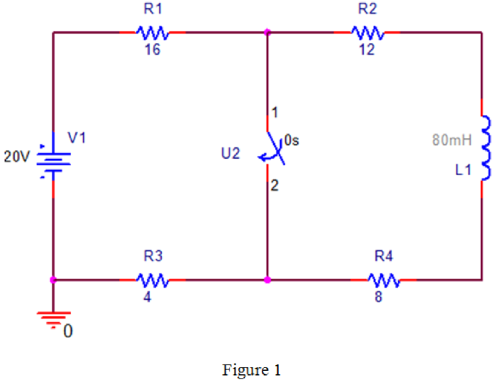
PSPICE Circuit:
Refer to Figure P7.1 in the textbook.
Draw the given circuit diagram in PSPICE as shown in Figure 1.
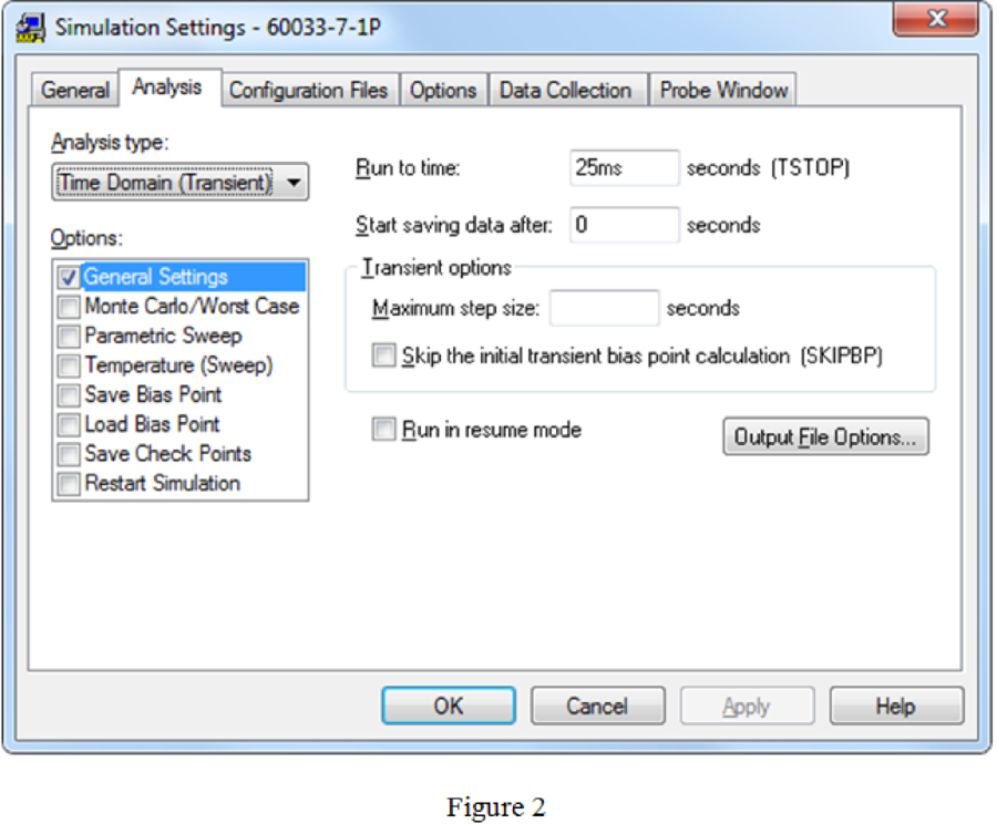
Simulation settings:
Provide the simulation settings as shown in Figure 2.
PSPICE output:
After run the PSPICE circuit a black output screen will be displayed. Right click on the mouse by keeping cursor on the output screen, click the option “Add Trace” and type the expression “I(L1)” in trace expression box.
The current plot
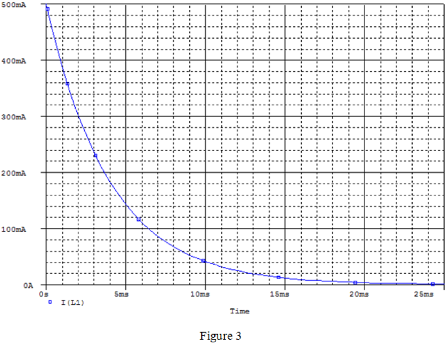
From PSPICE output, the initial and final value of output current is,
Conclusion:
Therefore, the current values
b)
Find the expression
b)
Answer to Problem 1P
The expression
Explanation of Solution
Calculation:
Find the equivalent resistance after the switch is closed at
Find time constant from the circuit diagram.
Here,
L is the inductance.
Substitute
The expression
Substitute
Conclusion:
Therefore, the expression
c)
Find the time taken to reach the output current of 100 mA after closed the switch.
c)
Answer to Problem 1P
The time required to reach 100 mA of output current is 6.4 ms.
Explanation of Solution
Calculation:
The expression of output current
Substitute 100 mA for
Conclusion:
Therefore, the time required to reach 100 mA of output current is 6.4 ms.
Want to see more full solutions like this?
Chapter 7 Solutions
EBK ELECTRIC CIRCUITS


- 1- Write the mesh equation for the circuit below. Solve the equations using Crame method (matrix and determinant), and find the current of resistor 4 ohm. 6 A www 10 Ω w 6Ω www 12 V + 402 www 12 Ω 2- Write the nodal equations for the circuit below. You do not need to solve the equation just write the matrix equation. R3 ww 8Ω R₁ 201 5 A 12 3A R₂40arrow_forwardPlease solve these 3 questions in detailarrow_forward1. Please draw the root locus by hand for the following closed-loop system, where G(s) s+8 S-2 and H(s) = Find the range of K for stability Input R(s) Output C(s) KG(s) H(s) s+6 = S-2arrow_forward
- The state-space Jordan Canonical Form of the following system is: Y(s) 8-5 U(s) (+1)(+3) Select one: O a. -1 0 0 A = 0 -1 0 B: ... ... ... 0 0 C [4 1.5 1.5], D=0 b. -3 1 0 0 A = 0 -3 0 1 B ... 0 0 -1 C -4 -1.5 1.5], D=0 ○ C. -3 1 0 A = 0 -3 0 1 ,B= ... 0 0 ○ d. C [4 1.5 1.5], D=0 -3 1 0 0 A = 0 -3 0 1 , B: ... ... 0 0 -1 C [4 1.5 1.5], D=0 -4 1 If= x and (0): = then 2(t) is: -4 0 Select one: a. x2(t)=4te2t O b. x2(t) = e2t+2te2t Oc. 2(t)=-4te-21 Od. 2(t) e2-2te-2 =arrow_forwardThree speech signals are TDM multiplexed with a high-quanty music signal. It each speech signal is sampled at 16 kHz and PCM quantized by 8 bits/sample, while the music signal is sampled at 64 kHz with the same PCM quantizer. 1. Draw the block diagram of this TDM. 2. Calculate the output bit rate of this TDM.arrow_forward3- For the network below determine the value of R for maximum power to R (use Thevenin equivalent) and determine the value of maximum power R₁ 1.2Ω E + 12 V I D 10 A R₂60 6Ω Rarrow_forward
- Please solve this problem in detail to understandarrow_forwardQ3: (40 Marks) Single phase full bridge voltage source inverter has an RLC load with R-1002, L-31.5mH and C=112µF. The inverter frequency is 60Hz and de input voltage is 220V. (a) Express the instantaneous load current in Fourier series to third harmonic. (b) Calculate the RMS load current at the fundamental frequency (n=1). (c) Calculate the load power due to fundamental component (n=1).arrow_forward12.3 Express each of the waveforms in Fig. P12.3 (on page 667) in terms of step functions and then determine its Laplace transform. [Recall that the ramp function is related to the step function by r(t − T) = (t − T) u(t − T).] Assume that all waveforms are zero for t<0. - - -arrow_forward
- Evaluate each of the following integraarrow_forwardWith the aid of suitable diagrams, describe the benefits that antenna arrays have over singleelement antennas, with their applicationsarrow_forwardExplain what is meant by an electric dipole antenna, sketch its radiation pattern, state itsdirectivity and describe its main applicationsarrow_forward
 Introductory Circuit Analysis (13th Edition)Electrical EngineeringISBN:9780133923605Author:Robert L. BoylestadPublisher:PEARSON
 Delmar's Standard Textbook Of ElectricityElectrical EngineeringISBN:9781337900348Author:Stephen L. HermanPublisher:Cengage Learning
 Programmable Logic ControllersElectrical EngineeringISBN:9780073373843Author:Frank D. PetruzellaPublisher:McGraw-Hill Education
 Fundamentals of Electric CircuitsElectrical EngineeringISBN:9780078028229Author:Charles K Alexander, Matthew SadikuPublisher:McGraw-Hill Education
 Electric Circuits. (11th Edition)Electrical EngineeringISBN:9780134746968Author:James W. Nilsson, Susan RiedelPublisher:PEARSON
 Engineering ElectromagneticsElectrical EngineeringISBN:9780078028151Author:Hayt, William H. (william Hart), Jr, BUCK, John A.Publisher:Mcgraw-hill Education,