Draw the major control devices of a programmable controller.
Answer to Problem 1SQ
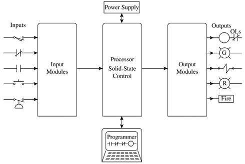
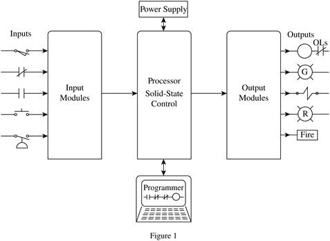
The major control devices of a programmable controller are as follows:
Explanation of Solution
Discussion:
A solid-state, electronic microprocessor-based control system is known as a programmable controller.
A programmable controller contains the following components.
- Power supply.
- Input modules.
- Processor.
- Output modules.
- Programmer.
The input devices such as push buttons, limit switches, and condition sensors are connected to input modules. The input module is monitored by the system to detect changes occurred in the input devices. Depending upon the status of input signals, the controller system reacts using user- programmed internal logic. The response obtained by the controller device is used to drive the output loads such as motor starter, control relays, contactors, and alarms.
The major control devices of a programmable controller are shown in Figure 1.
Conclusion:
Thus, major control devices of a programmable controller are shown in Figure 1.
Want to see more full solutions like this?
Chapter 58 Solutions
Electric Motor Control

- Please do question 3 and 4 of this question, the first part is submitted as a separate question due to the limit. Thank you, I will give positive feedback. Please explain each step clearlyarrow_forwardIf the circuit shown in Fig. P12.38(a) is excited by thecurrent waveform is(t) shown in Fig. P12.38(b), determine i(t)for t ≥ 0, given that R1 = 10 W, R2 = 5 W, and C = 0.02 F.arrow_forwardPlease explain each step clearly and include a proper image of what the block diagram and plot must look like. thank youarrow_forward
- A three-phase, 480-V, 60-Hz, 6-pole, Y-connected induction motor has its speed controlled by slip power. The circuit parameters are given: Rs=0.06 ohms, Rr=0.05 ohms, Xs=0.2 ohms, Xr=0.3 ohms and Xm=6 ohms. The turn ratio of the rotor to stator winding is n=0.8. The no-load losses of the motor are equal to 150 W. The rotor and stator cupper losses are equal to 249.21 W. The slip power losses are estimated to 8000W. The load torque is 173.61 N.m. at 700 rpm. The efficiency is equal to: Select one: a. 71.5% b. None of these c. 81.5% d. 91.5%arrow_forwardQuestion 1: A 3 phase, 10 kW, 1700 rpm, Y- connected 460 V, 60 Hz, 4 poles, Y-connected induction motor has the following parameters: Rr = 0.2 ohms, Xs = 0.8 ohms, Xr = 0.8 ohms, Xm = 20 ohms. The no load losses are neglected. The rotor speed is assumed to be constant equal to 1700 rpm. The V/F control method is applied. The stator resistance is negligible. If the base synchronous speed is 188.5 rad/s and the voltage frequency ratio is 1.405, then the maximum torque Tm and the corresponding speed w at 30 Hz are equal to: Select one: a. 350 N.m and 70.69 rad/s b. None of these c. 350 N.m and 164.94 rad/s d. 700 N.m and 164.94 rad/s Question 2: A 3 phase, 10 kW, 1750 rpm, Y- connected 460 V, 60 Hz, 4 poles, Y-connected induction motor has the following parameters: Rs = 0.5 Ohms, Rr = 0.3 Ohms, Xs = 0.9 Ohms, Xr = 0.9 Ohms, Xm = 25 Ohms. The no load losses are neglected. In this type of control the developed torque is proportional to the square of the statoric voltage. In this part, the…arrow_forwardPlease explain each question vlearly and explain how to do it. Thank you, I will give pos feedbackarrow_forward
- Don't use ai to answer I will report you answerarrow_forwardDon't use ai to answer I will report you answerarrow_forward12.43 For the circuit shown in Fig. P12.43, determine Vout (1) given that R₁ = 1 kQ, R₂ = 4k, and C = 1 μF, and (a) v(t)=2u(1) (V), (b) s(t)=2 cos(10001) (V), (c) vs(t) = 2e u(t) (V). R1 Us(1) + R2 Dout(1) Figure P12.43 Op-amp circuit for Problem 12.43.arrow_forward
- 12.41 The circuit shown in Fig. P12.41 was introduced in Problem 5.68. Then, a time-domain solution was sought for Dout, (1) and Dout₂ (1) for 10, given that v₁(1) = 10u(t) mV, Vcc 10 V for both op amps, and the two capacitors had no change prior to t = 0. Analyze the circuit and plot Dout, (t) and Dout (1) using the Laplace transform technique. 4μF 5 μF Οι 5 ΚΩ Dout 1 MQ Dout2 + Vcc = 10 V Vec = 10 V Figure P12.41 Circuit for Problems 12.41 and 12.42.arrow_forward12.38 If the circuit shown in Fig. P12.38(a) is excited by the current waveform is(t) shown in Fig. P12.38(b), determine i(t) for 1 > 0, given that R₁ = 102, R2 = 5 92, and C = 0.02 F. is(t) R₁ i(t) R₂ is(t) 1.5 A 1.5A | 1 A 0.5 A- M 0.5A- (a) Circuit www. (b) Waveform 0 = 4 rad/s t Figure P12.38 Circuit for Problems 12.38 to 12.40.arrow_forwardEXERCISE 1: Consider the waveguide of Example Calculate the phase constant, phase velocity and wave impedance for TE10 and TM11 modes at the operating frequency of 15 GHz. = 192.4 . For Answer: For TE10, B = 615.6 rad/m, u = 1.531 × 10⁸ m/s, TE 529.4 rad/m, u = 1.78 x 10 m/s, TM = 158.8 Q. TM11, B Example 1: A rectangular waveguide with dimensions a = 2.5 cm, b = 1 cm is to operate below 15.1 GHz. How many TE and TM modes can the waveguide transmit? if the guide is filled with a medium characterized by σ = 0, &=4&o Hr = 1° Calculate the cutoff frequencies of the modes.arrow_forward

 Electricity for Refrigeration, Heating, and Air C...Mechanical EngineeringISBN:9781337399128Author:Russell E. SmithPublisher:Cengage Learning