
Computer Science Illuminated
7th Edition
ISBN: 9781284155617
Author: Nell Dale, John Lewis
Publisher: Jones & Bartlett Learning
expand_more
expand_more
format_list_bulleted
Videos
Question
Chapter 4, Problem 60E
Program Plan Intro
Circuit:
- The circuit is known as the combination of gates that is used to achieve a difficult logical operation.
- It has two general categories; they are:
- Combinational circuit
- Sequential circuit
Expert Solution & Answer
Explanation of Solution
Given circuit diagram:
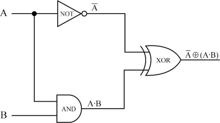
Behavior of the circuit:
- From the circuit diagram:
- First, the input A is passed to NOT gate to perform the inverse of the A and produces the output as
- Next, the input A and input B is passed in the AND gate to perform the product of A and B, to produce the output as
- Finally, the output of NOT gate and the output of AND gate is passed as the input of XOR gate.
- Note: when both the inputs are the same, then the output of XOR gate is 0. Otherwise, the output of XOR gate is 1.
- That is, “
- First, the input A is passed to NOT gate to perform the inverse of the A and produces the output as
Truth table for the given circuit diagram:
Step 1:
- The inputs are A and B for the above circuit diagram:
| A | B | |||
| 0 | 0 | |||
| 0 | 1 | |||
| 1 | 0 | |||
| 1 | 1 |
Step 2:
- When the inputs are A as 0 and B as 0:
| A | B | |||
| 0 | 0 | 1 | 0 | 1 |
| 0 | 1 | |||
| 1 | 0 | |||
| 1 | 1 |
- First, the input A as 0 is passed to NOT gate to perform the inverse of the A and produces the output as
- Next, the input A as 0 and input B as 0 is passed to the AND gate to perform the product of A and B and produce the output as
- Finally, the output of NOT gate and the output of AND gate is passed as the input of XOR gate.
- Note: when both the inputs are the same, then the output of XOR gate is 0. Otherwise, the output of XOR gate is 1.
- That is, “1” and “0” are passed as inputs to XOR gate and produces output as
Step 3:
- When the inputs are A as 0 and B as 1:
| A | B | |||
| 0 | 0 | 1 | 0 | 1 |
| 0 | 1 | 1 | 0 | 1 |
| 1 | 0 | |||
| 1 | 1 |
- First, the input A as 0 is passed to NOT gate to perform the inverse of the A and produces the output as
- Next, the input A as 0 and input B as 1 is passed to the AND gate to perform the product of the A and B and produce the output as
- Finally, the output of NOT gate and the output of AND gate is passed as the input of XOR gate.
- Note: when both the inputs are the same, then the output of XOR gate is 0. Otherwise, the output of XOR gate is 1.
- That is, “1” and “0” are passed as input for XOR gate and produce output as
Step 4:
- When the inputs are A as 1 and B as 0:
| A | B | |||
| 0 | 0 | 1 | 0 | 1 |
| 0 | 1 | 1 | 0 | 1 |
| 1 | 0 | 0 | 0 | 0 |
| 1 | 1 |
- First, the input A as 1 is passed to NOT gate to perform the inverse of A and produces the output as
- Next, the input A as 1 and input B as 0 is passed in the AND gate to perform the product of the A and B and produce the output as
- Finally, the output of NOT gate and the output of AND gate is passed as the input to XOR gate.
- Note: when both the inputs of XOR gate are the same, the output of XOR gate is 0. Otherwise, the output of XOR gate is 1.
- That is, “0” and “0” are passed as input for XOR gate and produce as the output
Step 5:
- When the inputs are A as 1 and B as 1:
| A | B | |||
| 0 | 0 | 1 | 0 | 1 |
| 0 | 1 | 1 | 0 | 1 |
| 1 | 0 | 0 | 0 | 0 |
| 1 | 1 | 0 | 1 | 1 |
- First, the input A as 1 is passed to NOT gate to perform the inverse of the A and produces the output as
- Next, the input A and input B as 1 is passed in the AND gate to perform the product of the A and B and produce the output as
- Finally, the output of NOT gate and the output of AND gate is passed as the input of XOR gate.
- Note: when both the inputs of XOR gate are the same, the output of XOR gate is 0. Otherwise, the output of XOR gate is 1.
- That is, “0” and “1” are passed as input for XOR gate and produce as the output
Final truth table:
Therefore, truth table of the given circuit diagram is:
| A | B | |||
| 0 | 0 | 1 | 0 | 1 |
| 0 | 1 | 1 | 0 | 1 |
| 1 | 0 | 0 | 0 | 0 |
| 1 | 1 | 0 | 1 | 1 |
Want to see more full solutions like this?
Subscribe now to access step-by-step solutions to millions of textbook problems written by subject matter experts!
Students have asked these similar questions
"Do not use AI tools. Solve the problem by hand on paper only and upload a photo of your handwritten solution."
| √ (r² + r + 1)e^ dr
Ensure you answer the question asked at the end of the document. Do not just paste things without the GNS3 console outputs
Chapter 4 Solutions
Computer Science Illuminated
Ch. 4 - Prob. 1ECh. 4 - Prob. 2ECh. 4 - Prob. 3ECh. 4 - Prob. 4ECh. 4 - Prob. 5ECh. 4 - Prob. 6ECh. 4 - Prob. 7ECh. 4 - Prob. 8ECh. 4 - Prob. 9ECh. 4 - Prob. 10E
Ch. 4 - Prob. 11ECh. 4 - Prob. 12ECh. 4 - Prob. 13ECh. 4 - Prob. 14ECh. 4 - Prob. 15ECh. 4 - Prob. 16ECh. 4 - Prob. 17ECh. 4 - Prob. 18ECh. 4 - Prob. 19ECh. 4 - Prob. 20ECh. 4 - Prob. 21ECh. 4 - Prob. 22ECh. 4 - Prob. 23ECh. 4 - Prob. 24ECh. 4 - Prob. 25ECh. 4 - Prob. 26ECh. 4 - Prob. 27ECh. 4 - Prob. 28ECh. 4 - Prob. 29ECh. 4 - Prob. 30ECh. 4 - Prob. 31ECh. 4 - Prob. 32ECh. 4 - Prob. 33ECh. 4 - Prob. 34ECh. 4 - Prob. 35ECh. 4 - Prob. 36ECh. 4 - Prob. 37ECh. 4 - Prob. 38ECh. 4 - Prob. 39ECh. 4 - Prob. 40ECh. 4 - Prob. 41ECh. 4 - Prob. 42ECh. 4 - Prob. 43ECh. 4 - Prob. 44ECh. 4 - Prob. 45ECh. 4 - Prob. 46ECh. 4 - Prob. 47ECh. 4 - Prob. 48ECh. 4 - Prob. 49ECh. 4 - Prob. 50ECh. 4 - Prob. 51ECh. 4 - Prob. 52ECh. 4 - Prob. 53ECh. 4 - Prob. 54ECh. 4 - Prob. 55ECh. 4 - Prob. 56ECh. 4 - Prob. 57ECh. 4 - Prob. 58ECh. 4 - Prob. 59ECh. 4 - Prob. 60ECh. 4 - Prob. 61ECh. 4 - Prob. 62ECh. 4 - Prob. 63ECh. 4 - Prob. 64ECh. 4 - Prob. 65ECh. 4 - Prob. 66ECh. 4 - Prob. 67ECh. 4 - Prob. 68ECh. 4 - Prob. 69ECh. 4 - Prob. 70ECh. 4 - Prob. 71ECh. 4 - Prob. 72ECh. 4 - Prob. 73ECh. 4 - Prob. 1TQCh. 4 - Prob. 2TQCh. 4 - Prob. 3TQCh. 4 - Prob. 4TQ
Knowledge Booster


Learn more about
Need a deep-dive on the concept behind this application? Look no further. Learn more about this topic, computer-science and related others by exploring similar questions and additional content below.Similar questions
- "Do not use AI tools. Solve the problem by hand on paper only and upload a photo of your handwritten solution."arrow_forward"Do not use AI tools. Solve the problem by hand on paper only and upload a photo of your handwritten solution."arrow_forward"Do not use AI tools. Solve the problem by hand on paper only and upload a photo of your handwritten solution."arrow_forward
- "Do not use AI tools. Solve the problem by hand on paper only and upload a photo of your handwritten solution."arrow_forwardSolve this "Do not use AI tools. Solve the problem by hand on paper only and upload a photo of your handwritten solution."arrow_forward"Do not use AI tools. Solve the problem by hand on paper only and upload a photo of your handwritten solution."arrow_forward
- "Do not use AI tools. Solve the problem by hand on paper only and upload a photo of your handwritten solution."arrow_forwardSpecifications: Part-1Part-1: DescriptionIn this part of the lab you will build a single operation ALU. This ALU will implement a bitwise left rotation. Forthis lab assignment you are not allowed to use Digital's Arithmetic components.IF YOU ARE FOUND USING THEM, YOU WILL RECEIVE A ZERO FOR LAB2!The ALU you will be implementing consists of two 4-bit inputs (named inA and inB) and one 4-bit output (named out). Your ALU must rotate the bits in inA by the amount given by inB (i.e. 0-15).Part-1: User InterfaceYou are provided an interface file lab2_part1.dig; start Part-1 from this file.NOTE: You are not permitted to edit the content inside the dotted lines rectangle. Part-1: ExampleIn the figure above, the input values that we have selected to test are inA = {inA_3, inA_2, inA_1, inA_0} = {0, 1, 0,0} and inB = {inB_3, inB_2, inB_1, inB_0} = {0, 0, 1, 0}. Therefore, we must rotate the bus 0100 bitwise left by00102, or 2 in base 10, to get {0, 0, 0, 1}. Please note that a rotation left is…arrow_forwardSolve this "Do not use AI tools. Solve the problem by hand on paper only and upload a photo of your handwritten solution."arrow_forward
- Solve this "Do not use AI tools. Solve the problem by hand on paper only and upload a photo of your handwritten solution."arrow_forward"Do not use AI tools. Solve the problem by hand on paper only and upload a photo of your handwritten solution."arrow_forwardSolve this "Do not use AI tools. Solve the problem by hand on paper only and upload a photo of your handwritten solution."arrow_forward
arrow_back_ios
SEE MORE QUESTIONS
arrow_forward_ios
Recommended textbooks for you
 Database System ConceptsComputer ScienceISBN:9780078022159Author:Abraham Silberschatz Professor, Henry F. Korth, S. SudarshanPublisher:McGraw-Hill Education
 Starting Out with Python (4th Edition)Computer ScienceISBN:9780134444321Author:Tony GaddisPublisher:PEARSON
 Digital Fundamentals (11th Edition)Computer ScienceISBN:9780132737968Author:Thomas L. FloydPublisher:PEARSON
 C How to Program (8th Edition)Computer ScienceISBN:9780133976892Author:Paul J. Deitel, Harvey DeitelPublisher:PEARSON
 Database Systems: Design, Implementation, & Manag...Computer ScienceISBN:9781337627900Author:Carlos Coronel, Steven MorrisPublisher:Cengage Learning
 Programmable Logic ControllersComputer ScienceISBN:9780073373843Author:Frank D. PetruzellaPublisher:McGraw-Hill Education
Database System Concepts
Computer Science
ISBN:9780078022159
Author:Abraham Silberschatz Professor, Henry F. Korth, S. Sudarshan
Publisher:McGraw-Hill Education
Starting Out with Python (4th Edition)
Computer Science
ISBN:9780134444321
Author:Tony Gaddis
Publisher:PEARSON
Digital Fundamentals (11th Edition)
Computer Science
ISBN:9780132737968
Author:Thomas L. Floyd
Publisher:PEARSON
C How to Program (8th Edition)
Computer Science
ISBN:9780133976892
Author:Paul J. Deitel, Harvey Deitel
Publisher:PEARSON
Database Systems: Design, Implementation, & Manag...
Computer Science
ISBN:9781337627900
Author:Carlos Coronel, Steven Morris
Publisher:Cengage Learning
Programmable Logic Controllers
Computer Science
ISBN:9780073373843
Author:Frank D. Petruzella
Publisher:McGraw-Hill Education
Boolean Algebra - Digital Logic and Logic Families - Industrial Electronics; Author: Ekeeda;https://www.youtube.com/watch?v=u7XnJos-_Hs;License: Standard YouTube License, CC-BY
Boolean Algebra 1 – The Laws of Boolean Algebra; Author: Computer Science;https://www.youtube.com/watch?v=EPJf4owqwdA;License: Standard Youtube License