EBK THE ANALYSIS AND DESIGN OF LINEAR C
8th Edition
ISBN: 9781119140320
Author: Toussaint
Publisher: VST
expand_more
expand_more
format_list_bulleted
Videos
Textbook Question
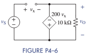
Chapter 4, Problem 4.6P
Find the voltage gain
Expert Solution & Answer
Want to see the full answer?
Check out a sample textbook solution
Students have asked these similar questions
Calculate the value for V1, V2 and V3
Prelab Information
Laboratory Preliminary Discussion
Second-order RLC Circuit Analysis
The second-order RLC circuit shown in figure 1 below represents all voltages and impedances as functions of the complex
variable, s. Note, of course, that the impedances associated with R, RL, and Rs are constant independent of frequency, so the 's'
notation is omitted. Again, one of the advantages of s-domain analysis is that we can apply all of the circuit analysis techniques
learned for AC and DC circuits.
ZI(s)
Zc(s)
Rs
w
RL
ww
+
+
VRS(S)
VRL(S)
VL(s)
Vc(s)
VR(S)
R
Vs(s)
Figure 1: A second-order RLC circuit represented in the s-domain.
To generate the s-domain expression for the output voltage, Vout(s) = VR(S), for the circuit shown in figure 1, we can apply voltage
division in the s-domain as shown in equation 1 below. For equation 1 we define the following circuit parameters.
RT=RS + RL + R where: R₁ = Total series resistance
Rs Signal generator output resistance (fixed)
Inductor internal…
5.137
The BJT in the circuit of Fig. 5.137 has ẞ = 100.
(a) Find the de collector current and the de
voltage at the collector.
(b) Replacing the transistor by its T model,
draw the small-signal equivalent circuit of the
amplifier. Analyze the resulting circuit to
determine the voltage gain vo/vi.
V
ww
0.3 mA
300 ΚΩ
=
250 Ω
Va
30 ΚΩ
www||
Fig. 5.137
Chapter 4 Solutions
EBK THE ANALYSIS AND DESIGN OF LINEAR C
Ch. 4 - Find the voltage gain vO/vS and current gain iO/ix...Ch. 4 - Prob. 4.2PCh. 4 - Prob. 4.3PCh. 4 - Prob. 4.4PCh. 4 - Find the voltage gain vO/vS in Figure P4-5.Ch. 4 - Find the voltage gain vO/vS in Figure P4-6.Ch. 4 - Find an expression for the current gain iO/iS in...Ch. 4 - Prob. 4.8PCh. 4 - Prob. 4.9PCh. 4 - Find an expression for the voltage gain vO/vs in...
Ch. 4 - Prob. 4.12PCh. 4 - In the circuit of Figure P4-13, the VCVS has of...Ch. 4 - Prob. 4.14PCh. 4 - (a) Find the Thévenin equivalent circuit that the...Ch. 4 - Prob. 4.16PCh. 4 - Prob. 4.18PCh. 4 - Prob. 4.19PCh. 4 - The circuit parameters in figure P4-21 are...Ch. 4 - The circuit parameters in Figure P4-21 are...Ch. 4 - The parameters of the transistor in Figure P4-23...Ch. 4 - Prob. 4.25PCh. 4 - Find the voltage gain of each OP AMP circuit shown...Ch. 4 - Considering simplicity and standard 10 tolerance...Ch. 4 - Two OP AMP circuits are shown in Figure P4-28....Ch. 4 - Prob. 4.29PCh. 4 - What is the range of the gain vO/vS in Figure...Ch. 4 - Using only one OP AMP, design a circuit that...Ch. 4 - Design a circuit using only one OP AMP that...Ch. 4 - Prob. 4.36PCh. 4 - For the circuit in Figure P4-37: (a) Find vO in...Ch. 4 - A young designer needed to amplify a 2-V signal by...Ch. 4 - Design two circuits to produce the following...Ch. 4 - Design a noninverting summer for five inputs with...Ch. 4 - For the circuit in Figure P4-41: Find vO in terms...Ch. 4 - The input-output relationship for a three-input...Ch. 4 - Find vo in terms of the inputs v1,v2, and v3 in...Ch. 4 - Prob. 4.44PCh. 4 - Prob. 4.45PCh. 4 - Prob. 4.46PCh. 4 - Prob. 4.47PCh. 4 - It is claimed that vO=vS when the switch is closed...Ch. 4 - Prob. 4.49PCh. 4 - Prob. 4.50PCh. 4 - Use node-voltage analysis in Figure P4-51 to show...Ch. 4 - Prob. 4.52PCh. 4 - Prob. 4.53PCh. 4 - For the block diagram of Figure P4-54: Find an...Ch. 4 - For the block diagram of Figure P4-55: Find an...Ch. 4 - For the circuit in Figure P4-56: Find vO in terms...Ch. 4 - Prob. 4.57PCh. 4 - Onan exam, students were asked to design an...Ch. 4 - Prob. 4.59PCh. 4 - For the circuit of Figure P4-60: Use node-voltage...Ch. 4 - Prob. 4.61PCh. 4 - Design a single OP AMP amplifier with a voltage...Ch. 4 - Design an OP AMP amplifier with a voltage gain of...Ch. 4 - Using a single OP AMP, design a circuit with...Ch. 4 - Design a differential amplifier with inputs v1 and...Ch. 4 - Using no more than two OP AMPs, design an OP AMP...Ch. 4 - Design a two-input noninverting summer that will...Ch. 4 - Design a three-input noninverting summer that will...Ch. 4 - Design a cascaded OP AMP circuit that will produce...Ch. 4 - Design a cascaded OP AMP circuit that will produce...Ch. 4 - Using the instrumentation amplifier shown in...Ch. 4 - Prob. 4.73PCh. 4 - Design a circuit that can produce vO=2000vTR2.6V...Ch. 4 - A requirement exists for an OP AMP circuit with...Ch. 4 - A requirement exists for an OP AMP circuit to...Ch. 4 - A particular application requires that an...Ch. 4 - Prob. 4.78PCh. 4 - The full-scale output of a six-bit DAC is 10.0 V....Ch. 4 - An R2R DAC is shown in Figure P4-80. The digital...Ch. 4 - A fifth bit is added to the R-2R DAC shown in...Ch. 4 - Prob. 4.82PCh. 4 - Prob. 4.83PCh. 4 - A small pressure transducer has the...Ch. 4 - A medical grade pressure transducer has been...Ch. 4 - The acid/alkaline balance of a fluid is measured...Ch. 4 - A photoresistor varies from 10 in bright sunlight...Ch. 4 - Your engineering firm needs an instrumentation...Ch. 4 - Prob. 4.90PCh. 4 - Prob. 4.92PCh. 4 - Prob. 4.93PCh. 4 - A five-bit flash ADC in Figure P4-94 uses a...Ch. 4 - Bipolar Power Supply Voltages The circuit in...Ch. 4 - Thermometer Design Problem There is a need to...Ch. 4 - High Bias Design Problem A particular pressure...Ch. 4 - Prob. 4.99IPCh. 4 - OP AMP Circuit Analysis and Design Find the...Ch. 4 - Instrumentation Amplifier with Alarm Strain gauges...
Knowledge Booster


Learn more about
Need a deep-dive on the concept behind this application? Look no further. Learn more about this topic, electrical-engineering and related others by exploring similar questions and additional content below.Similar questions
- solve this, show all steps, no ai pz, please draw it outarrow_forwardNO AI PLEASE WILL REJECTarrow_forward"?Can the expert help me solve only a bonus question using Arduino" The system must control 3 LEDs (Red, Green, and Blue) to operate in 4 different lighting modes: Mode 3: LEDs fade in and out smoothly (PWM control) in the order Red Green → Blue. Bonus Challenge (Potentiometer Control): The potentiometer (connected to pin A0) allows for dynamic control of the brightness during the fading mode (Mode 3). This allows the user to adjust how bright or dim the LEDs should fade in and out. This solution meets the project requirements, including the current limits, and provides interactive functionality with the push button and potentiometer.arrow_forward
- See the attached image for answeringarrow_forwardI need a complete and correct solution, please Suppose that X and Y have the following joint probability distribution y 24 1 [0.1 0.15] P(X,Y) = x3 0.2 0.3 50.1 0.15] a) Evaluate the marginal distribution of X and Y b) Find P(Y/X) and P(X/Y). c) Find P(Y=2/X=3). d) Find μx, Hy, σ,σ and oxy.arrow_forwardSuppose that X and Y have the following joint probability distribution 2 1 [0.1 y 4 0.151 P(X,Y) = x3 0.2 0.3 50.1 0.15 a) Evaluate the marginal distribution of X and Y. b) Find P(Y/X) and P(X/Y). c) Find P(Y=2/X=3). d) Find μx, μy, σ,σ and oxy.arrow_forward
- Prelab Information Laboratory Preliminary Discussion Second-order RLC Circuit Analysis The second-order RLC circuit shown in figure 1 below represents all voltages and impedances as functions of the complex variable, s. Note, of course, that the impedances associated with R, RL, and Rs are constant independent of frequency, so the 's' notation is omitted. Again, one of the advantages of s-domain analysis is that we can apply all of the circuit analysis techniques learned for AC and DC circuits. ZI(s) Zc(s) Rs w RL ww + + VRS(S) VRL(S) VL(s) Vc(s) VR(S) R Vs(s) Figure 1: A second-order RLC circuit represented in the s-domain. To generate the s-domain expression for the output voltage, Vout(s) = VR(S), for the circuit shown in figure 1, we can apply voltage division in the s-domain as shown in equation 1 below. For equation 1 we define the following circuit parameters. RT=RS + RL + R where: R₁ = Total series resistance Rs Signal generator output resistance (fixed) Inductor internal…arrow_forwardCan you show how the correct answer was found.arrow_forwardFor the circuit shown in Figure (1). Solve the following: ( A. What type of logic does it represent? C. Explain the function of D1. B. What type of logic family does it belong to? D. Explain the importance of DL. E. How many stages it has? Explain the function of each one. F. Construct the truth table and explain it briefly. G.How can you convert this circuit to an open collector form? Explain and sketch it. H.How can you convert this circuit to a tri-state form? Explain and sketch it. I. How can you prevent the transistors from being saturated? J. Which transistor should be modified to convert this circuit to a 4-inputs NAND? Explain and sketch it. K.Convert this circuit to a 2-inputs NOR gate and draw it. R-1200 R-4.2K R-1.5K R-IK Figure (1) lour e Yourarrow_forward
- E. How many stages it has? Explain the function of each one. F. Construct the truth table and explain it briefly. G.How can you convert this circuit to an open collector form? Explain and sketch it. H.How can you convert this circuit to a tri-state form? Explain and sketch it. I. How can you prevent the transistors from being saturated? J. Which transistor should be modified to convert this circuit to a 4-inputs NAND? Explain and sketch it. K.Convert this circuit to a 2-inputs NOR gate and draw it. R-4.2K W R-1200 R-1.5K R-IK Figure (1) JOUT e Yourarrow_forward1. Determine the z-transform, including the region of convergence (ROC), of the following signals: a)x[n={3,0,0,0,0,51-4} b) x2[n] = ((1/3)^n ,n ≥0 2", n < 0 c) X3[n]= (1/3)^n- 2", n ≥ 0 0, n < 0arrow_forwardUse ECL configuration to realize a 2-inputs OR /NOR gate and verify its function using the truth table, showing the state of each transistor in the circuit. Assume Vcc 5V, VEE-0V & VREF=1.5V.arrow_forward
arrow_back_ios
SEE MORE QUESTIONS
arrow_forward_ios
Recommended textbooks for you
 Introductory Circuit Analysis (13th Edition)Electrical EngineeringISBN:9780133923605Author:Robert L. BoylestadPublisher:PEARSON
 Delmar's Standard Textbook Of ElectricityElectrical EngineeringISBN:9781337900348Author:Stephen L. HermanPublisher:Cengage Learning
 Programmable Logic ControllersElectrical EngineeringISBN:9780073373843Author:Frank D. PetruzellaPublisher:McGraw-Hill Education
 Fundamentals of Electric CircuitsElectrical EngineeringISBN:9780078028229Author:Charles K Alexander, Matthew SadikuPublisher:McGraw-Hill Education
 Electric Circuits. (11th Edition)Electrical EngineeringISBN:9780134746968Author:James W. Nilsson, Susan RiedelPublisher:PEARSON
 Engineering ElectromagneticsElectrical EngineeringISBN:9780078028151Author:Hayt, William H. (william Hart), Jr, BUCK, John A.Publisher:Mcgraw-hill Education,
Introductory Circuit Analysis (13th Edition)
Electrical Engineering
ISBN:9780133923605
Author:Robert L. Boylestad
Publisher:PEARSON
Delmar's Standard Textbook Of Electricity
Electrical Engineering
ISBN:9781337900348
Author:Stephen L. Herman
Publisher:Cengage Learning
Programmable Logic Controllers
Electrical Engineering
ISBN:9780073373843
Author:Frank D. Petruzella
Publisher:McGraw-Hill Education
Fundamentals of Electric Circuits
Electrical Engineering
ISBN:9780078028229
Author:Charles K Alexander, Matthew Sadiku
Publisher:McGraw-Hill Education
Electric Circuits. (11th Edition)
Electrical Engineering
ISBN:9780134746968
Author:James W. Nilsson, Susan Riedel
Publisher:PEARSON
Engineering Electromagnetics
Electrical Engineering
ISBN:9780078028151
Author:Hayt, William H. (william Hart), Jr, BUCK, John A.
Publisher:Mcgraw-hill Education,
Boost Converters and Buck Converters: Power Electronics; Author: Physics Videos by Eugene Khutoryansky;https://www.youtube.com/watch?v=vwJYIorz_Aw;License: Standard Youtube License