EBK THE ANALYSIS AND DESIGN OF LINEAR C
8th Edition
ISBN: 9781119140320
Author: Toussaint
Publisher: VST
expand_more
expand_more
format_list_bulleted
Videos
Textbook Question
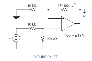
Chapter 4, Problem 4.37P
For the circuit in Figure P4-37:
(a) Find
(b) Find
Expert Solution & Answer
Want to see the full answer?
Check out a sample textbook solution
Students have asked these similar questions
electric plants
do hand writing
please solve quickly. thank you!
Please show all steps
Chapter 4 Solutions
EBK THE ANALYSIS AND DESIGN OF LINEAR C
Ch. 4 - Find the voltage gain vO/vS and current gain iO/ix...Ch. 4 - Prob. 4.2PCh. 4 - Prob. 4.3PCh. 4 - Prob. 4.4PCh. 4 - Find the voltage gain vO/vS in Figure P4-5.Ch. 4 - Find the voltage gain vO/vS in Figure P4-6.Ch. 4 - Find an expression for the current gain iO/iS in...Ch. 4 - Prob. 4.8PCh. 4 - Prob. 4.9PCh. 4 - Find an expression for the voltage gain vO/vs in...
Ch. 4 - Prob. 4.12PCh. 4 - In the circuit of Figure P4-13, the VCVS has of...Ch. 4 - Prob. 4.14PCh. 4 - (a) Find the Thévenin equivalent circuit that the...Ch. 4 - Prob. 4.16PCh. 4 - Prob. 4.18PCh. 4 - Prob. 4.19PCh. 4 - The circuit parameters in figure P4-21 are...Ch. 4 - The circuit parameters in Figure P4-21 are...Ch. 4 - The parameters of the transistor in Figure P4-23...Ch. 4 - Prob. 4.25PCh. 4 - Find the voltage gain of each OP AMP circuit shown...Ch. 4 - Considering simplicity and standard 10 tolerance...Ch. 4 - Two OP AMP circuits are shown in Figure P4-28....Ch. 4 - Prob. 4.29PCh. 4 - What is the range of the gain vO/vS in Figure...Ch. 4 - Using only one OP AMP, design a circuit that...Ch. 4 - Design a circuit using only one OP AMP that...Ch. 4 - Prob. 4.36PCh. 4 - For the circuit in Figure P4-37: (a) Find vO in...Ch. 4 - A young designer needed to amplify a 2-V signal by...Ch. 4 - Design two circuits to produce the following...Ch. 4 - Design a noninverting summer for five inputs with...Ch. 4 - For the circuit in Figure P4-41: Find vO in terms...Ch. 4 - The input-output relationship for a three-input...Ch. 4 - Find vo in terms of the inputs v1,v2, and v3 in...Ch. 4 - Prob. 4.44PCh. 4 - Prob. 4.45PCh. 4 - Prob. 4.46PCh. 4 - Prob. 4.47PCh. 4 - It is claimed that vO=vS when the switch is closed...Ch. 4 - Prob. 4.49PCh. 4 - Prob. 4.50PCh. 4 - Use node-voltage analysis in Figure P4-51 to show...Ch. 4 - Prob. 4.52PCh. 4 - Prob. 4.53PCh. 4 - For the block diagram of Figure P4-54: Find an...Ch. 4 - For the block diagram of Figure P4-55: Find an...Ch. 4 - For the circuit in Figure P4-56: Find vO in terms...Ch. 4 - Prob. 4.57PCh. 4 - Onan exam, students were asked to design an...Ch. 4 - Prob. 4.59PCh. 4 - For the circuit of Figure P4-60: Use node-voltage...Ch. 4 - Prob. 4.61PCh. 4 - Design a single OP AMP amplifier with a voltage...Ch. 4 - Design an OP AMP amplifier with a voltage gain of...Ch. 4 - Using a single OP AMP, design a circuit with...Ch. 4 - Design a differential amplifier with inputs v1 and...Ch. 4 - Using no more than two OP AMPs, design an OP AMP...Ch. 4 - Design a two-input noninverting summer that will...Ch. 4 - Design a three-input noninverting summer that will...Ch. 4 - Design a cascaded OP AMP circuit that will produce...Ch. 4 - Design a cascaded OP AMP circuit that will produce...Ch. 4 - Using the instrumentation amplifier shown in...Ch. 4 - Prob. 4.73PCh. 4 - Design a circuit that can produce vO=2000vTR2.6V...Ch. 4 - A requirement exists for an OP AMP circuit with...Ch. 4 - A requirement exists for an OP AMP circuit to...Ch. 4 - A particular application requires that an...Ch. 4 - Prob. 4.78PCh. 4 - The full-scale output of a six-bit DAC is 10.0 V....Ch. 4 - An R2R DAC is shown in Figure P4-80. The digital...Ch. 4 - A fifth bit is added to the R-2R DAC shown in...Ch. 4 - Prob. 4.82PCh. 4 - Prob. 4.83PCh. 4 - A small pressure transducer has the...Ch. 4 - A medical grade pressure transducer has been...Ch. 4 - The acid/alkaline balance of a fluid is measured...Ch. 4 - A photoresistor varies from 10 in bright sunlight...Ch. 4 - Your engineering firm needs an instrumentation...Ch. 4 - Prob. 4.90PCh. 4 - Prob. 4.92PCh. 4 - Prob. 4.93PCh. 4 - A five-bit flash ADC in Figure P4-94 uses a...Ch. 4 - Bipolar Power Supply Voltages The circuit in...Ch. 4 - Thermometer Design Problem There is a need to...Ch. 4 - High Bias Design Problem A particular pressure...Ch. 4 - Prob. 4.99IPCh. 4 - OP AMP Circuit Analysis and Design Find the...Ch. 4 - Instrumentation Amplifier with Alarm Strain gauges...
Knowledge Booster


Learn more about
Need a deep-dive on the concept behind this application? Look no further. Learn more about this topic, electrical-engineering and related others by exploring similar questions and additional content below.Similar questions
- 12-3) PDF, mean, & variance A random variable has the PDF shown in the figure. a) Find the numerical value of the parameter K. b) Write the numerical expression for the PDF. c) Find the probability that the random variable is negative. d) Find the mean of x, the expected value of x², and the variance of x. K Px(x) 3 Xarrow_forwardPlease show all stepsarrow_forward12-4) Gaussian random variable A Gaussian random variable has a mean value of 4 and a standard deviation of 3. Find the probability that the value of the random variable exceeds 16. Repeat for the probability that it is less than -2. The discussion of Marcum's Q function given in the lecture notes may be helpful.arrow_forward
- A transformer has a primary voltage of 240 V and a secondary voltage of 48 V. What is the turns ratio of this transformer?arrow_forwardmicroprocers and microcontrolerarrow_forwardDesign a counter to count-up from 2 to 7 using three of D Flip Flops (3) 3-Bit Count up (3 to 5) Using D Flip-Flop: The State Equation of D Flip-Flop: Q(t+1)=D(t) => Dn=Qn Present State D Flip-Flop Next State n Q2p Q1p Q0p 3 0 1 1 1 Q2n Q1n Q0n D2 D1 D0 0 0 1 0 0 4 1 0 0 1 0 1 1 0 1 5 1 0 1 0 1 1 01 1 D2-Sum(3,4) and don't care X-Sum(0,1,2,6,7) D1=Sum(5) and don't care X=Sum(0,1,2,6,7) D0=Sum(4,5) and don't care X=Sum(0,1,2,6,7) Using K-map to simplify the functions: D2=Q1+Q0' D1=Q1'QO DO=Q1' XOX XOX Q2 10 Q2 01 Q2 1xx Q0 QO Qo D2 Q2 >CK Q2 D1 Q1 BCD CK Q1 DO QF ►CK Q0 ☐ Present State Next State D Flip-Flop n Q2p Q1p Q0p Q2n Q1n Q0n D2 D1 D0 2 0 1 0 0 1 1 0 1 1 3 0 1 1 1 0 0 1 00 4 1 0 0 1 0 1 1 0 1 5 1 0 1 1 1 0 1 1 0 6 1 1 0 0 1 0 0 1 0 D2 D2=Sum(3,4,5), X=Sum(0,1,7) D1 Q2 1 Q1 1 0 ☑ 0 Qo D2=Q0+Q1' ✗ 0 Q1arrow_forward
- Consider the following 4×1 multiplexer with inputs: w0=2, w1=1, w2=x2' and w3=0 And with switches: S1 x1 and S0=x0 What is the multiplexer output f as a function of x2, x1 and x0?arrow_forwardI need help adding a capacitor and a Zener diode to my circuit. I’m looking for a simple sketch or diagram showing how to connect them. i want diagram with final circuit after adding the zener diad and capacitor. don't do calclution or anything. thanksarrow_forwardQuestion 3 AC Motor Drives [15]Calculate the instantaneous currents delivered by the inverter if the direct axiscurrent required at a particular instant is 8.66A and the quadrature current is5A. Derive all equations for the three currents.arrow_forward
- A certain signal f(t) has the following PSD (assume 12 load): Sp (w) = new + 8(w) - 1.5) + (w + 1.5)] (a) What is the mean power in the bandwidth w≤2 rad/see? (b) What is the mean power in the bandwidth -1.9 to 0.99 rad/sec? Paress(w) dw 2ㅈ -arrow_forward(75 Marks) JA signal (t) is bond 7)(t)(t) and f(t), are band-limited to 1.2 kHz each. These signals are to be limited to 9.6 kHz, and three other signals transmitted by means of time-division multiplexing. Set up scheme for accomplishing this multiplexing requirement, with each signal sampled at its Nyquist rate. What must be the speed of the commutator (the output but ram-k bit/sec)? the minimum band width? (25 Marks)arrow_forwardDraw the digital modulation outputs, ASK Amplitude Shift Keying) FSK (Frequency Shift Keying) and PSK (Phase Shift Keying). For baseband and carriet frequency as shown 101 wwwwwwwwwwww 010 BASESAND basband CARRIER Carralarrow_forward
arrow_back_ios
SEE MORE QUESTIONS
arrow_forward_ios
Recommended textbooks for you
 Introductory Circuit Analysis (13th Edition)Electrical EngineeringISBN:9780133923605Author:Robert L. BoylestadPublisher:PEARSON
 Delmar's Standard Textbook Of ElectricityElectrical EngineeringISBN:9781337900348Author:Stephen L. HermanPublisher:Cengage Learning
 Programmable Logic ControllersElectrical EngineeringISBN:9780073373843Author:Frank D. PetruzellaPublisher:McGraw-Hill Education
 Fundamentals of Electric CircuitsElectrical EngineeringISBN:9780078028229Author:Charles K Alexander, Matthew SadikuPublisher:McGraw-Hill Education
 Electric Circuits. (11th Edition)Electrical EngineeringISBN:9780134746968Author:James W. Nilsson, Susan RiedelPublisher:PEARSON
 Engineering ElectromagneticsElectrical EngineeringISBN:9780078028151Author:Hayt, William H. (william Hart), Jr, BUCK, John A.Publisher:Mcgraw-hill Education,
Introductory Circuit Analysis (13th Edition)
Electrical Engineering
ISBN:9780133923605
Author:Robert L. Boylestad
Publisher:PEARSON
Delmar's Standard Textbook Of Electricity
Electrical Engineering
ISBN:9781337900348
Author:Stephen L. Herman
Publisher:Cengage Learning
Programmable Logic Controllers
Electrical Engineering
ISBN:9780073373843
Author:Frank D. Petruzella
Publisher:McGraw-Hill Education
Fundamentals of Electric Circuits
Electrical Engineering
ISBN:9780078028229
Author:Charles K Alexander, Matthew Sadiku
Publisher:McGraw-Hill Education
Electric Circuits. (11th Edition)
Electrical Engineering
ISBN:9780134746968
Author:James W. Nilsson, Susan Riedel
Publisher:PEARSON
Engineering Electromagnetics
Electrical Engineering
ISBN:9780078028151
Author:Hayt, William H. (william Hart), Jr, BUCK, John A.
Publisher:Mcgraw-hill Education,
Lead and lag compensation using Bode diagrams; Author: John Rossiter;https://www.youtube.com/watch?v=UBE-Tp173vk;License: Standard Youtube License