Digital Fundamentals (11th Edition)
11th Edition
ISBN: 9780132737968
Author: Thomas L. Floyd
Publisher: PEARSON
expand_more
expand_more
format_list_bulleted
Videos
Textbook Question
Chapter 3, Problem 1P
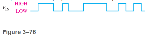
The input waveform shown in Figure 3-76 is applied to an inverter. Draw the timing diagram of the output waveform in proper relation to the input.
Expert Solution & Answer
Want to see the full answer?
Check out a sample textbook solution
Students have asked these similar questions
Suppose your computer is responding very slowly to information requests from the Internet. You observe that your network gateway shows high levels of network activity even though you have closed your e-mail client, Web browser, and all other programs that access the Internet.
What types of malwares could cause such symptoms? What steps can you take to check whether malware has gained access to your system? What tools can you use at each step? If you identify malware, what ways might it have entered your system? How can you restore your PC to safe operation, including the special software tools you may use?
R language
Using R language
Chapter 3 Solutions
Digital Fundamentals (11th Edition)
Ch. 3.1 - When a 1 is on the input of an inverter, what is...Ch. 3.1 - An active-HIGH pulse (HIGH level when asserted,...Ch. 3.2 - When is the output of an AND gate HIGH?Ch. 3.2 - When is the output of an AND gate LOW?Ch. 3.2 - Describe the truth table for a 5-input AND gate.Ch. 3.3 - When is the output of an OR gate HIGH?Ch. 3.3 - When is the output of an OR gate LOW?Ch. 3.3 - Describe the truth table for a 3-input OR gate.Ch. 3.4 - When is the output of a NAND gate LOW?Ch. 3.4 - When is the output of a NAND gate HIGH?
Ch. 3.4 - Describe the functional differences between a NAND...Ch. 3.4 - Write the output expression for a NAND gate with...Ch. 3.5 - When is the output of a NOR gate HIGH?Ch. 3.5 - When is the output of a NOR gate LOW?Ch. 3.5 - Describe the functional difference between a NOR...Ch. 3.5 - Write the output expression for a 3-input NOR with...Ch. 3.6 - When is the output of an XOR gate HIGH?Ch. 3.6 - When is the output of an XNOR gate HIGH?Ch. 3.6 - How can you use an XOR gate to detect when two...Ch. 3.7 - List six process technologies used for...Ch. 3.7 - What does the term volatile mean in relation to...Ch. 3.7 - What are two design entry methods for programming...Ch. 3.7 - Prob. 4CUCh. 3.7 - Write a VHDL description of a 3-input NOR gate,Ch. 3.7 - Write a VHDL description of an XOR gate.Ch. 3.8 - How is fixed-function logic different than PLD...Ch. 3.8 - Prob. 2CUCh. 3.8 - Identify the following IC logic designators: LS HC...Ch. 3.8 - Prob. 4CUCh. 3.8 - What does the term hex inverter mean? What does...Ch. 3.8 - A positive pulse is applied to an inverter input....Ch. 3.8 - A certain gate has a propagation delay time of 6...Ch. 3.8 - Prob. 8CUCh. 3.8 - Prob. 9CUCh. 3.8 - Prob. 10CUCh. 3.9 - Prob. 1CUCh. 3.9 - If two different input waveforms are applied to a...Ch. 3.9 - Prob. 3CUCh. 3 - An inverter performs the NOR operation.Ch. 3 - An AND gate can have only two inputsCh. 3 - If any input to an OR is 1, the output is 1.Ch. 3 - If all inputs to an AND gate are 1, the output is...Ch. 3 - A NAND gate has an output that is opposite the...Ch. 3 - A NOR gate can be considered as an OR gate...Ch. 3 - The output of an exclusive-OR is 0 if the inputs...Ch. 3 - Prob. 8TFQCh. 3 - Once programmed, PLD logic can be changed.Ch. 3 - Fan-out is the number of similar gates that a...Ch. 3 - When the input to an inverter is HIGH (1), the...Ch. 3 - An inverter performs an operation known as...Ch. 3 - The output of an AND gate with inputs A, B, and C...Ch. 3 - The output of an OR gate with inputs A, B, and C...Ch. 3 - A pulse is applied to each input of a 2-input NAND...Ch. 3 - A pulse is applied to each input of a 2-input NOR...Ch. 3 - A pulse is applied to each input of an...Ch. 3 - Prob. 8STCh. 3 - The purpose of a programmable link in an AND array...Ch. 3 - The term OTP means open test point one-time...Ch. 3 - Prob. 11STCh. 3 - Prob. 12STCh. 3 - Two ways to enter a logic design using PLD...Ch. 3 - Prob. 14STCh. 3 - In-system programming of a PLD typically utilizes...Ch. 3 - To measure the period of a pulse waveform, you...Ch. 3 - Prob. 17STCh. 3 - The input waveform shown in Figure 3-76 is applied...Ch. 3 - A combination of inverters is shown in Figure...Ch. 3 - If the waveform in Figure 3-76 is applied to point...Ch. 3 - Draw the rectangular outline symbol for a 4-input...Ch. 3 - Determine the output, X, for a 2-input AND gate...Ch. 3 - Repeat problem 5 for the waveforms in Figure 3-79Ch. 3 - The input wave forms applied to a 3-input AND gate...Ch. 3 - The input waveforms applied to a 4-input AND gate...Ch. 3 - Draw the rectangular outline symbol for a 3-input...Ch. 3 - Write the expression for a 5-input OR gate with...Ch. 3 - Determine the output for a 2-input OR gate when...Ch. 3 - Repeat Problem 7 for a 3-input OR gate.Ch. 3 - Repeat Problem 8 for a 4-input OR gate.Ch. 3 - For the five input waveforms in Figure 3-8219,...Ch. 3 - Draw the rectangular outline symbol for a 4-input...Ch. 3 - Show the truth table for a 3-input OR gate.Ch. 3 - For the set of input waveforms in Figure 3-83,...Ch. 3 - Determine the gate output for the input waveforms...Ch. 3 - Determine the output waveform in Figure 3-8513Ch. 3 - As you have learned, the two logic symbols shown...Ch. 3 - Repeat Problem 17 for a 2-input NOR gate.Ch. 3 - Determine the output waveform in Figure 3-87 and...Ch. 3 - Repeat Problem 19 for a 4-input NOR gate.Ch. 3 - The NAND and the negative-OR symbols represent...Ch. 3 - How does an exclusive-OR gate differ from an OR...Ch. 3 - Repeat Problem 17 for an exclusive-OR gate.Ch. 3 - Repeat Problem 17 for an exclusive-NOR gateCh. 3 - Determine the output of an exclusive-OR gate for...Ch. 3 - In the simple programmed AND array with...Ch. 3 - Determine by row and column number which fusible...Ch. 3 - Describe a 4-input AND gate using VHDL.Ch. 3 - Describe a 5-input NOR gate using VHDLCh. 3 - In the comparison of certain logic devices, it is...Ch. 3 - Prob. 34PCh. 3 - Determine tPLHandtPHL from the oscilloscope...Ch. 3 - Prob. 36PCh. 3 - If a logic gate operates on a dc supply voltage of...Ch. 3 - The variable ICCH represents the dc supply current...Ch. 3 - Examine the conditions indicated in Figure 3-92,...Ch. 3 - Determine the faulty gates in Figure 3-93 by...Ch. 3 - Using an oscilloscope, you make the observations...Ch. 3 - Prob. 42PCh. 3 - Every time the ignition switch is turned on in the...Ch. 3 - What failure(s) would you suspect if the output of...Ch. 3 - Modify the frequency counter in Figure 3-16 to...Ch. 3 - Prob. 46PCh. 3 - Design a circuit to fit in the beige block of...Ch. 3 - Modify the logic circuit for the intrusion alarm...Ch. 3 - Further modify the logic circuit from Problem 48...Ch. 3 - Sensors are used to monitor the pressure and the...Ch. 3 - In a certain automated manufacturing process,...Ch. 3 - Open file P03-52. For the specified fault, predict...Ch. 3 - Open file P03-53. For the specified fault, predict...Ch. 3 - Open file P03-54. For the observed behavior...Ch. 3 - Open file P03-55. For the observed behavior...
Additional Engineering Textbook Solutions
Find more solutions based on key concepts
This optional Google account security feature sends you a message with a code that you must enter, in addition ...
SURVEY OF OPERATING SYSTEMS
Explain forward-only cursors. Give an example of their use.
Database Concepts (8th Edition)
Why is it important for a program to close an open file as soon as it is done using the file? Give two reasons.
Starting Out with C++: Early Objects (9th Edition)
Porter’s competitive forces model: The model is used to provide a general view about the firms, the competitors...
Management Information Systems: Managing The Digital Firm (16th Edition)
The Whi1e loop is a ______ type of loop. a. pretest b. posttest c. prequalified d. post iterative
Starting Out with Programming Logic and Design (5th Edition) (What's New in Computer Science)
What is the general problem with static scoping?
Concepts Of Programming Languages
Knowledge Booster


Learn more about
Need a deep-dive on the concept behind this application? Look no further. Learn more about this topic, computer-science and related others by exploring similar questions and additional content below.Similar questions
- Compare the security services provided by a digital signature (DS) with those of a message authentication code (MAC). Assume that Oscar can observe all messages sent between Rina and Naseem. Oscar has no knowledge of any keys but the public one, in the case of DS. State whether DS and MAC protect against each attack and, if they do, how. The value auth(x) is computed with a DS or a MAC algorithm. In each scenario, assume the message M = x#####auth(x). (Message integrity) Rina has the textual data x = “Transfer $1000 to Mark” to send to Naseem. To ensure the integrity of the data, Rina generates auth(x), forms a message M, and then sends M in cleartext to Naseem. Oscar intercepts the message and replaces “Mark” with “Oscar.” Will Naseem detect this in the case of either DS or MAC? If yes, how will Naseem detect it? If not, why? (Replay) Rina has the textual data x = “Transfer $1000 to Mark” to send to Naseem. To ensure the integrity of the data, Rina generates auth(x), forms a message…arrow_forwardI need to resolve the following....You are trying to convince your boss that your company needs to invest in a license for MS-Project (project management software from Microsoft) before beginning a systems project. What arguments would you give her?arrow_forwardWhat are the four types of feasibility? what is the issues addressed by each feasibility component.arrow_forward
- I would like to get ab example of a situation where Agile Methods might be preferable versus the traditional SDLC? What are the characteristics of this situation that give Agile Methods an advantage?arrow_forwardWhat is a functional decomposition diagram? what is a good example of a high level task being broken down into tasks in at least two lower levels (three levels in all).arrow_forwardWhat are the advantages to using a Sytems Analysis and Design model like the SDLC vs. other approaches?arrow_forward
- 3. Problem Description: Define the Circle2D class that contains: Two double data fields named x and y that specify the center of the circle with get methods. • A data field radius with a get method. • A no-arg constructor that creates a default circle with (0, 0) for (x, y) and 1 for radius. • A constructor that creates a circle with the specified x, y, and radius. • A method getArea() that returns the area of the circle. • A method getPerimeter() that returns the perimeter of the circle. • • • A method contains(double x, double y) that returns true if the specified point (x, y) is inside this circle. See Figure (a). A method contains(Circle2D circle) that returns true if the specified circle is inside this circle. See Figure (b). A method overlaps (Circle2D circle) that returns true if the specified circle overlaps with this circle. See the figure below. р O со (a) (b) (c)< Figure (a) A point is inside the circle. (b) A circle is inside another circle. (c) A circle overlaps another…arrow_forward1. Explain in detail with examples each of the following fundamental security design principles: economy of mechanism, fail-safe default, complete mediation, open design, separation of privilege, least privilege, least common mechanism, psychological acceptability, isolation, encapsulation, modularity, layering, and least astonishment.arrow_forwardSecurity in general means the protection of an asset. In the context of computer and network security, explore and explain what assets must be protected within an online university. What the threats are to the security of these assets, and what countermeasures are available to mitigate and protect the organization from such threats. For each of the assets you identify, assign an impact level (low, moderate, or high) for the loss of confidentiality, availability, and integrity. Justify your answers.arrow_forward
- Please include comments and docs comments on the program. The two other classes are Attraction and Entertainment.arrow_forwardObject-Oriented Programming In this separate files. ent, you'll need to build and run a small Zoo in Lennoxville. All classes must be created in Animal (5) First, start by building a class that describes an Animal at a Zoo. It should have one private instance variable for the name of the animal, and one for its hunger status (fed or hungry). Add methods for setting and getting the hunger satus variable, along with a getter for the name. Consider how these should be named for code clarity. For instance, using a method called hungry () to make the animal hungry could be used as a setter for the hunger field. The same logic could be applied to when it's being fed: public void feed () { this.fed = true; Furthermore, the getter for the fed variable could be named is Fed as it is more descriptive about what it answers when compared to get Fed. Keep this technique in mind for future class designs. Zoo (10) Now we have the animals designed and ready for building a little Zoo! Build a class…arrow_forward1.[30 pts] Answer the following questions: a. [10 pts] Write a Boolean equation in sum-of-products canonical form for the truth table shown below: A B C Y 0 0 0 1 0 0 1 0 0 1 0 0 0 1 1 0 1 0 0 1 1 0 1 0 1 1 0 1 1 1 1 0 a. [10 pts] Minimize the Boolean equation you obtained in (a). b. [10 pts] Implement, using Logisim, the simplified logic circuit. Include an image of the circuit in your report. 2. [20 pts] Student A B will enjoy his picnic on sunny days that have no ants. He will also enjoy his picnic any day he sees a hummingbird, as well as on days where there are ants and ladybugs. a. Write a Boolean equation for his enjoyment (E) in terms of sun (S), ants (A), hummingbirds (H), and ladybugs (L). b. Implement in Logisim, the logic circuit of E function. Use the Circuit Analysis tool in Logisim to view the expression, include an image of the expression generated by Logisim in your report. 3.[20 pts] Find the minimum equivalent circuit for the one shown below (show your work): DAB C…arrow_forward
arrow_back_ios
SEE MORE QUESTIONS
arrow_forward_ios
Recommended textbooks for you
 Systems ArchitectureComputer ScienceISBN:9781305080195Author:Stephen D. BurdPublisher:Cengage Learning
 Operations Research : Applications and AlgorithmsComputer ScienceISBN:9780534380588Author:Wayne L. WinstonPublisher:Brooks Cole
 EBK JAVA PROGRAMMINGComputer ScienceISBN:9781305480537Author:FARRELLPublisher:CENGAGE LEARNING - CONSIGNMENT
 Principles of Information Systems (MindTap Course...Computer ScienceISBN:9781285867168Author:Ralph Stair, George ReynoldsPublisher:Cengage Learning
 Programming Logic & Design ComprehensiveComputer ScienceISBN:9781337669405Author:FARRELLPublisher:Cengage
 Fundamentals of Information SystemsComputer ScienceISBN:9781337097536Author:Ralph Stair, George ReynoldsPublisher:Cengage Learning
Systems Architecture
Computer Science
ISBN:9781305080195
Author:Stephen D. Burd
Publisher:Cengage Learning
Operations Research : Applications and Algorithms
Computer Science
ISBN:9780534380588
Author:Wayne L. Winston
Publisher:Brooks Cole
EBK JAVA PROGRAMMING
Computer Science
ISBN:9781305480537
Author:FARRELL
Publisher:CENGAGE LEARNING - CONSIGNMENT
Principles of Information Systems (MindTap Course...
Computer Science
ISBN:9781285867168
Author:Ralph Stair, George Reynolds
Publisher:Cengage Learning
Programming Logic & Design Comprehensive
Computer Science
ISBN:9781337669405
Author:FARRELL
Publisher:Cengage
Fundamentals of Information Systems
Computer Science
ISBN:9781337097536
Author:Ralph Stair, George Reynolds
Publisher:Cengage Learning
Boolean Algebra - Digital Logic and Logic Families - Industrial Electronics; Author: Ekeeda;https://www.youtube.com/watch?v=u7XnJos-_Hs;License: Standard YouTube License, CC-BY
Boolean Algebra 1 – The Laws of Boolean Algebra; Author: Computer Science;https://www.youtube.com/watch?v=EPJf4owqwdA;License: Standard Youtube License