Concept explainers
Videos
a.
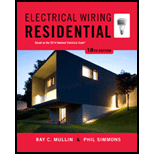
Draw the correct symbol for the description “Lighting panel”.
a.
Explanation of Solution
The symbol for the lighting panel is drawn and it is shown in Figure 1 as follows:
Conclusion:
Thus, the symbol for the given description is drawn.
b.
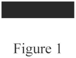
Draw the correct symbol for the description “Clock outlet”.
b.
Explanation of Solution
The symbol for the clock outlet is drawn and it is shown in Figure 2 as follows:
Conclusion:
Thus, the symbol for the given description is drawn.
c.
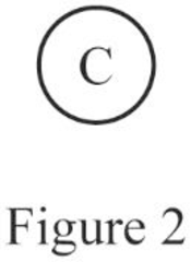
Draw the correct symbol for the description “Duplex outlet”.
c.
Explanation of Solution
The symbol for the duplex outlet is drawn and it is shown in Figure 3 as follows:
Conclusion:
Thus, the symbol for the given description is drawn.
d.
Draw the correct symbol for the description “Outside telephone”.
d.
Explanation of Solution
The symbol for the outside telephone is drawn and it is shown in Figure 4 as follows:

Conclusion:
Thus, the symbol for the given description is drawn.
e.
Draw the correct symbol for the description “Single-pole switch”.
e.
Explanation of Solution
The symbol for the single-pole switch is drawn and it is shown in Figure 5 as follows:
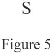
Conclusion:
Thus, the symbol for the given description is drawn.
f.
Draw the correct symbol for the description “Motor”.
f.
Explanation of Solution
The symbol for the motor is drawn and it is shown in Figure 6 as follows:
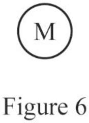
Conclusion:
Thus, the symbol for the given description is drawn.
g.
Draw the correct symbol for the description “Duplex outlet, split-wired”.
g.
Explanation of Solution
The symbol for the duplex outlet, split-wired is drawn and it is shown in Figure 7 as follows:
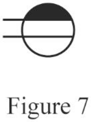
Conclusion:
Thus, the symbol for the given description is drawn.
h.
Draw the correct symbol for the description “Lampholder with pull switch”.
h.
Explanation of Solution
The symbol for the lampholder with pull switch is drawn and it is shown in Figure 8 as follows:

Conclusion:
Thus, the symbol for the given description is drawn.
i.
Draw the correct symbol for the description “Weatherproof outlet”.
i.
Explanation of Solution
The symbol for the weatherproof outlet is drawn and it is shown in Figure 9 as follows:
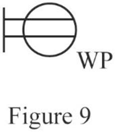
Conclusion:
Thus, the symbol for the given description is drawn.
j.
Draw the correct symbol for the description “Special-purpose outlet”.
j.
Explanation of Solution
The symbol for the special-purpose outlet is drawn and it is shown in Figure 10 as follows:
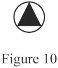
Conclusion:
Thus, the symbol for the given description is drawn.
k.
Draw the correct symbol for the description “fan outlet”.
k.
Explanation of Solution
The symbol for the fan outlet is drawn and it is shown in Figure 11 as follows:
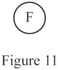
Conclusion:
Thus, the symbol for the given description is drawn.
l.
Draw the correct symbol for the description “Range outlet”.
l.
Explanation of Solution
The symbol for the range outlet is drawn and it is shown in Figure 12 as follows:
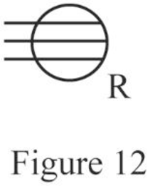
Conclusion:
Thus, the symbol for the given description is drawn.
m.
Draw the correct symbol for the description “Power panel”.
m.
Explanation of Solution
The symbol for the power panel is drawn and it is shown in Figure 13 as follows:
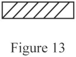
Conclusion:
Thus, the symbol for the given description is drawn.
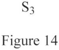
n.
Draw the correct symbol for the description “3-way switch”.
n.
Explanation of Solution
The symbol for the 3-way switch is drawn and it is shown in Figure 14 as follows:
Conclusion:
Thus, the symbol for the given description is drawn.
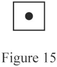
o.
Draw the correct symbol for the description “Push button”.
o.
Explanation of Solution
The symbol for the push button is drawn and it is shown in Figure 15 as follows:
Conclusion:
Thus, the symbol for the given description is drawn.
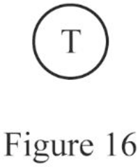
p.
Draw the correct symbol for the description “Thermostat”.
p.
Explanation of Solution
The symbol for the thermostat is drawn and it is shown in Figure 16 as follows:
Conclusion:
Thus, the symbol for the given description is drawn.
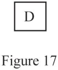
q.
Draw the correct symbol for the description “Electric door opener”.
q.
Explanation of Solution
The symbol for the electric door opener is drawn and it is shown in Figure 17 as follows:
Conclusion:
Thus, the symbol for the given description is drawn.
r.
Draw the correct symbol for the description “Multioutlet assembly”.
r.
Explanation of Solution
The symbol for the multioutlet assembly is drawn and it is shown in Figure 18 as follows:
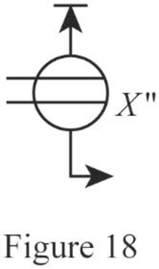
Where,
Conclusion:
Thus, the symbol for the given description is drawn.
Want to see more full solutions like this?
Chapter 2 Solutions
Electrical Wiring Residential


- 5. Sketch the root locus for L(s) = s+10 using rules 1, 2, and 4. For rule 4, you need to s(s+6) find the break-in and break-away points.arrow_forwardS+4 4. Sketch the root locus for L(s) = (s+6) (s+1)2 using rules 1, 2, and 3. For rule 3, you need to find the value of σ and a for the asymptotes. From the root-locus, explain why the closed-loop system is always stable for any choice of the design parameter K in the range 0 < K < ∞o.arrow_forward2. Consider the following system. K(s+3) (s+4) (s+1)(s+2) Check whether the points below are in the root locus. If the point is in the root locus, then also find what the corresponding gain K. i) ii) -2+j3 -2+1√ √ Hint: First find L(s). Next, in L(s) replace s with the value of the point and then express it in polar format r20 using calculator. The point will be in the root locus if and only if = 180° or odd multiple of 180°. When the point is in the root locus, the corresponding gain K is obtained as K ==arrow_forward
- 2. For each of the following transfer functions, G(s) = Y(s)/U(s), find the differential equation relating the input u(t) to the output y(t). (s+2)(s+3) (a) G(s) = (s+1)(s+4) (s²+0.4s+1.04) (s+3) (b) G(s)= (s2+0.2s+1)(s+2)(s+4)arrow_forwardDon't use ai to answer I will report you answerarrow_forward5. A schematic diagram of a motor connected to a load by gears is shown. Both the motor and the load are modeled as rotating masses with viscous damping. Find the transfer functions Øm/Tm and ØL/Tm. bm Jm Tm 0m N₂ N₁ OL но JL b₁arrow_forward
 EBK ELECTRICAL WIRING RESIDENTIALElectrical EngineeringISBN:9781337516549Author:SimmonsPublisher:CENGAGE LEARNING - CONSIGNMENT