
Verify whether the interconnection in the circuit in Figure P2.1 in the textbook is valid or not. Calculate the power developed by the current sources if the circuit is valid. Explain the reason if the interconnection in the circuit is not valid.

Answer to Problem 1P
The interconnection in the given circuit is valid and the power developed by the current sources is 1700 W.
Explanation of Solution
Given data:
Refer to Figure P2.1 in the textbook for required data.
Formula used:
Write the expression for power developed by the source (voltage or current) as follows:
Here,
Calculation:
From the given circuit, it is clear that, the voltage drop across the 10 A current source is 100 V and the voltage drop from the negative terminal of the 40 V voltage source to the bottom terminal of the 5 A current source must be 100 V.
In order to maintain the voltage drop of 100 V from the negative terminal of the 40 V voltage source to the bottom terminal of the 5 A current source the voltage drop across 5 A current source must be 140 V.
From the analysis, redraw the circuit as shown in Figure 1.
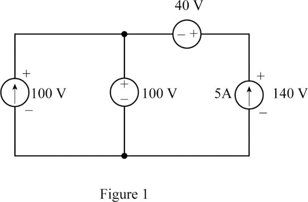
All the sources in the given circuit are independent sources. The independent voltage source can carry any current that required by the connection and the independent current source can support any voltage that required by the connection.
From the analysis, the voltage drop across the sources is satisfied. Therefore, the interconnection in the given circuit is valid.
Rewrite the expression in Equation (1) to find the power developed by the 10 A current source as follows:
From Figure 1, current 10 A enters from the negative terminal of 100 V. Therefore, the values of
The negative sign indicates the delivered power by the source. Therefore, the power developed by the 10 A current source is 1000 W.
Rewrite the expression in Equation (1) to find the power developed by the 5 A current source as follows:
From Figure 1, current 5 A enters from the negative terminal of 140 V. Therefore, the values of
As the negative sign indicates the delivered power by the source, the power developed by the 5 A current source 700 W.
Write the expression for power developed by the both current sources as follows:
Substitute 1000 W for
Conclusion:
Thus, the interconnection in the given circuit is valid and the power developed by the current sources is 1700 W.
Want to see more full solutions like this?
Chapter 2 Solutions
Electric Circuits. (11th Edition)
- Assume a JFET device with VGS(0) = -1.3 and ipss = 20 mA. Design a self-biased (Fig. 2) JFET common-source amplifier with the gain of -2 and a DC biasing that allows the largest swing in ip. Note that you can choose Vcc to arrive at a desired RD to meet the gain requirement. Since you are designing for a given gain, you may have to check to see if JFET is biased correctly. (Hint: First find Rs for correct VGs and then use the gain to compute RD. Finally, use RD and Rs to determine Vec). Assume that the amplifier is to interface a source that expects a load of 50 2. Also, assume that the amplifier circuit is AC coupled at both ends with 3 dB corner frequency of 15 kHz.arrow_forwardhelp on this question about induction motors?arrow_forwardThe MATLAB code is going well but the last part in bandpass, the legend that is supposed to tell the color of both lower and upper-frequency cutoff does not align with each other. As such I need help My Matlab code: % Define frequency range for the plot f = logspace(1, 5, 500); % Frequency range from 10 Hz to 100 kHz w = 2 * pi * f; % Angular frequency % Parameters for the filters R = 1e3; % Resistance in ohms (1 kΩ) C = 1e-6; % Capacitance in farads (1 μF) L = 0.1; % Inductance in henries (chosen for proper bandpass response) % Compute cutoff frequencies f_cutoff_RC = 1 / (2 * pi * R * C); % RC low-pass/high-pass cutoff f_resonance = 1 / (2 * pi * sqrt(L * C)); % Resonant frequency of RLC Q_factor = (1/R) * sqrt(L/C); % Quality factor of the circuit % Band-pass filter cutoff frequencies f_lower_cutoff = f_resonance / (sqrt(1 + 1/(4*Q_factor^2)) + 1/(2*Q_factor)); f_upper_cutoff = f_resonance / (sqrt(1 + 1/(4*Q_factor^2)) - 1/(2*Q_factor)); % Define Transfer Functions H_low =…arrow_forward
- The MATLAB code is going well but the last part in bandpass, the legend that is supposed to tell the color of both lower and upper-frequency cutoff does not align with each other. As such I need help My Matlab code: % Define frequency range for the plot f = logspace(1, 5, 500); % Frequency range from 10 Hz to 100 kHz w = 2 * pi * f; % Angular frequency % Parameters for the filters R = 1e3; % Resistance in ohms (1 kΩ) C = 1e-6; % Capacitance in farads (1 μF) L = 0.1; % Inductance in henries (chosen for proper bandpass response) % Compute cutoff frequencies f_cutoff_RC = 1 / (2 * pi * R * C); % RC low-pass/high-pass cutoff f_resonance = 1 / (2 * pi * sqrt(L * C)); % Resonant frequency of RLC Q_factor = (1/R) * sqrt(L/C); % Quality factor of the circuit % Band-pass filter cutoff frequencies f_lower_cutoff = f_resonance / (sqrt(1 + 1/(4*Q_factor^2)) + 1/(2*Q_factor)); f_upper_cutoff = f_resonance / (sqrt(1 + 1/(4*Q_factor^2)) - 1/(2*Q_factor)); % Define Transfer Functions H_low =…arrow_forward1° ⑤ Aa "Human-written solution required" 2. Using the characteristics of Fig. 6.11, determine ID for the following levels of VGs (with VDS > VP): a. VGs = 0V. b. VGs=-1 V. c. VGs -1.5 V. d. VGS -1.8 V. e. VGS = -4 V. f. VGs=-6V. 3. Using the results of problem 2 plot the transfer characteristics of ID vs. VGS- 4. a. Determine Vps for VGs = 0V and Ip = 6 mA using the characteristics of Fig. 6.11. b. Using the results of part (a), calculate the resistance of the JFET for the region Ip = 0 to 6 mA for VGs =0V. c. Determine Vps for VGS = -1 V and ID = 3 mA. d. Using the results of part (c), calculate the resistance of the JFET for the region ID = 0 to 3 mA for VGs -1 V. e. Determine Vps for VGs = -2 V and ID = 1.5 mA. f. Using the results of part (e), calculate the resistance of the JFET for the region ID = 0 to 1.5 mA for VGS-2 V. g. Defining the result of part (b) as ro, determine the resistance for VGs -1 V using Eq. (6.1) and compare with the results of part (d). h. Repeat part (g)…arrow_forward① Esterfication + R'on R Hydrolysis OH Alcohol A. 0-R Carboxylic Acid Ester NOD-10arrow_forward
- 4. a. Determine VDs for VGS = 0 V and ID = 6 mA using the characteristics of Fig. 6.11. b. Using the results of part (a), calculate the resistance of the JFET for the region ID = 0 to 6 mA for VGS = 0 V. c. Determine VDs for VGS = -1 V and ID = 3 mA. d. Using the results of part (c), calculate the resistance of the JFET for the region ID = 0 to 3 mA for VGS = -1 V. e. Determine VDs for VGS = -2 V and ID = 1.5 mA. f. Using the results of part (e), calculate the resistance of the JFET for the region ID = 0 to 1.5 mA for VGS = -2 V. g. Defining the result of part (b) as ro, determine the resistance for VGS = -1 V using Eq. (6.1) and compare with the results of part (d). h. Repeat part (g) for VGS = -2 V using the same equation, and compare the results with part (f). i. Based on the results of parts (g) and (h), does Eq. (6.1) appear to be a valid approximation?arrow_forwardA. Using D flip-flops, design a logic circuit for the finite-state machine described by the state assigned table in Fig. 1. Present Next State State Output x=0 x=1 Y2Y1 Y2Y1 YY Z 00 00 01 0 01 10 11 888 00 10 0 00 10 1 00 10 1 Fig. 1arrow_forwardAthree phase a.c. distributor AB has: A B C The distance from A to B is 500 m. The distance from A to C is 800 m. The impedance of each section is (6+j 8) /km. The voltage at the far end is maintained at 250 volt. Find: sending voltage, sending current, supply power factor and 80A 60 A total voltage drop. 0.8 lag. P.f 0.6 lead. p.farrow_forward
- engineering electromagnetics Subjectarrow_forwarda ADI ADI b Co ADDS D Fig.(2) 2-For resistive load, measure le output voltage by using oscilloscope; then sketch this wave. 3- Measure the average values ::f V₁ and IL: 4- Repeat steps 2 & 3 but for PL load.arrow_forwardDetermine the type of media In a certain medium with µ = o, & = 40 H = 12ely sin(x x 10% - By) a, A/m A plane wave propagating through a medium with ɛ, = 8, μ, = 2 has E = 0.5 3sin(10°t - Bz) a, V/m. Determine In a certain medium - E = 10 cos (2 x 10't ẞx)(a, + a.) V/m If μ == 50μo, & = 2ɛ, and o = 0, In a medium, -0.05x E=16e sin (2 x 10% -2x) a₂ V/marrow_forward
- Introductory Circuit Analysis (13th Edition)Electrical EngineeringISBN:9780133923605Author:Robert L. BoylestadPublisher:PEARSONDelmar's Standard Textbook Of ElectricityElectrical EngineeringISBN:9781337900348Author:Stephen L. HermanPublisher:Cengage LearningProgrammable Logic ControllersElectrical EngineeringISBN:9780073373843Author:Frank D. PetruzellaPublisher:McGraw-Hill Education
- Fundamentals of Electric CircuitsElectrical EngineeringISBN:9780078028229Author:Charles K Alexander, Matthew SadikuPublisher:McGraw-Hill EducationElectric Circuits. (11th Edition)Electrical EngineeringISBN:9780134746968Author:James W. Nilsson, Susan RiedelPublisher:PEARSONEngineering ElectromagneticsElectrical EngineeringISBN:9780078028151Author:Hayt, William H. (william Hart), Jr, BUCK, John A.Publisher:Mcgraw-hill Education,


