
Concept explainers
(a)
The value of output voltage,
(a)
Answer to Problem 61E
The value of output voltage,
Explanation of Solution
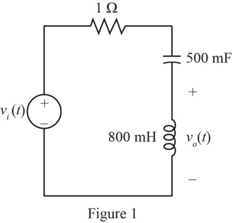
Given data:
The input voltage is,
The given diagram is shown in Figure 1.
Calculation:
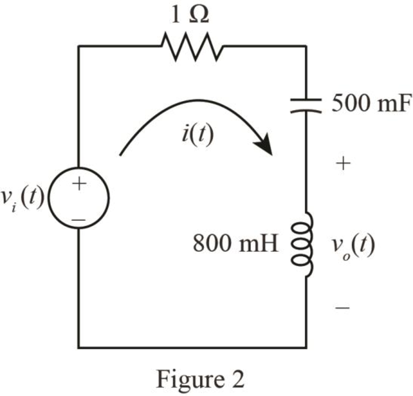
Mark the loop current
The required diagram is shown in Figure 2.
The conversion of
The conversion of
Hence, the value of the inductor,
The conversion of
The conversion of
Hence, the value of the capacitor,
The expression for output voltage using KVL is given by,
Substitute
Apply Fourier transform to the above expression.
The Fourier transform of
Substitute
Further solve as,
Apply shifting property for
Further solve as,
The inverse Fourier transform for the
The inverse Fourier transform for the
The inverse Fourier transform for the
Substitute
The expression for the output voltage from the figure is given by,
Substitute
Further solve as,
Conclusion:
Therefore, the value of output voltage,
(b)
The value of output voltage,
(b)
Answer to Problem 61E
The value of output voltage,
Explanation of Solution
Given data:
The input voltage is,
Calculation:
The expression for output voltage using KVL is given by,
Substitute
Apply Fourier transform to the above expression.
The Fourier transform of
Substitute
Further solve as,
The inverse Fourier transform for the
The inverse Fourier transform for the
Substitute
The expression for the output voltage from the figure is given by,
Substitute
Further solve as,
Conclusion:
Therefore, the value of output voltage,
Want to see more full solutions like this?
Chapter 17 Solutions
Engineering Circuit Analysis


- P 4.4-21 Determine the values of the node voltages V1, V2, and v3 for the circuit shown in Figure P 4.4-21. 29 ww 12 V +51 Aia ww 22. +21 ΖΩ www ΖΩ w +371 ①1 1 Aarrow_forward1. What is the theoretical attenuation of the output voltage at the resonant frequency? Answer to within 1%, or enter 0, or infinity (as “inf”) Attenuation =arrow_forwardWhat is the settling time for your output signal (BRF_OUT)? For this question, We define the settling time as the period of time it has taken for the output to settle into a steady state - ie when your oscillation first decays (aka reduces) to less than approximately 1/20 (5%) of the initial value. (a) Settling time = 22 μs Your last answer was interpreted as follows: Incorrect answer. Check 22 222 What is the peak to peak output voltage (BRF_OUT pp) at the steady state condition? You may need to use the zoom function to perform this calculation. Select a time point that is two times the settling time you answered in the question above. Answer to within 10% accuracy. (a) BRF_OUT pp= mVpp As you may have noticed, the output voltage amplitude is a tiny fraction of the input voltage, i.e. it has been significantly attenuated. Calculate the attenuation (decibels = dB) in the output signal as compared to the input based on the formula given below. Answer to within 1% accuracy.…arrow_forward
- my previous answers for a,b,d were wrong a = 1050 b = 950 d=9.99 c was the only correct value i got previously c = 100hz is correctarrow_forwardV₁(t) ww ZRI ZLI ZL2 ZTH Zci VTH Zc21 Figure 8. Circuit diagram showing calculation approach for VTH and Z TH we want to create a blackbox for the red region, we want to use the same input signal conditions as previously the design of your interference ector circuit: Sine wave with a 1 Vpp, with a frequency of 100 kHz (interference) Square wave with 2.4Vpp, with a frequency of 10 kHz (signal) member an AC Thevenin equivalent is only valid at one frequency. We have chosen to calculate the Thevenin equivalent circuit (and therefore the ackbox) at the interference frequency (i.e. 100 kHz), and the signal frequency (i.e. 10 kHz) as these are the key frequencies to analyse. Your boss is assured you that the waveform converter module has been pre-optimised to the DAB Receiver if you use the recommended circuit topology.arrow_forwardVs(t) + v(t) + vi(t) ZR ZL Figure 1: Second order RLC circuit Zc + ve(t) You are requested to design the circuit shown in Figure 1. The circuit is assumed to be operating at its resonant frequency when it is fed by a sinusoidal voltage source Vs (t) = 2sin(le6t). To help design your circuit you have been given the value of inductive reactance ZL = j1000. Assume that the amplitude of the current at resonance is Is (t) = 2 mA. Based on this information, answer the following to help design your circuit. Use cartesian notation for your answers, where required.arrow_forward
- What is the attenuation at the resonant frequency? You should use the LTSpice cursors for your measurement. Answer to within 1% accuracy, or enter 0, or infinity (as "inf") (a) Attenuation (dB) = dB Check You may have noticed that it was significantly easier to use frequency-domain "AC" simulation to measure the attenuation, compared to the steps we performed in the last few questions. (i.e. via a time-domain "transient" simulation). AC analysis allows us to observe and quantify large scale positive or negative changes in a signal of interest across a wide range of different frequencies. From the response you will notice that only frequencies that are relatively close to 100 kHz have been attenuated. This is the result of the Band-reject filter you have designed, and shows the 'rejection' (aka attenuation) of any frequencies that lie in a given band. The obvious follow-up question is how do we define this band? We use a quantity known as the bandwidth. A commonly used measurement for…arrow_forwardV₁(t) ww ZRI ZLI ZL2 ZTH Zci VTH Zc21 Figure 8. Circuit diagram showing calculation approach for VTH and Z TH we want to create a blackbox for the red region, we want to use the same input signal conditions as previously the design of your interference ector circuit: Sine wave with a 1 Vpp, with a frequency of 100 kHz (interference) Square wave with 2.4Vpp, with a frequency of 10 kHz (signal) member an AC Thevenin equivalent is only valid at one frequency. We have chosen to calculate the Thevenin equivalent circuit (and therefore the ackbox) at the interference frequency (i.e. 100 kHz), and the signal frequency (i.e. 10 kHz) as these are the key frequencies to analyse. Your boss is assured you that the waveform converter module has been pre-optimised to the DAB Receiver if you use the recommended circuit topology.arrow_forwardVs(t) + v(t) + vi(t) ZR ZL Figure 1: Second order RLC circuit Zc + ve(t) You are requested to design the circuit shown in Figure 1. The circuit is assumed to be operating at its resonant frequency when it is fed by a sinusoidal voltage source Vs (t) = 2sin(le6t). To help design your circuit you have been given the value of inductive reactance ZL = j1000. Assume that the amplitude of the current at resonance is Is (t) = 2 mA. Based on this information, answer the following to help design your circuit. Use cartesian notation for your answers, where required.arrow_forward
- For a band-rejection filter, the response drops below this half power point at two locations as visualised in Figure 7, we need to find these frequencies. Let's call the lower frequency-3dB point as fr and the higher frequency -3dB point fH. We can then find out the bandwidth as f=fHfL, as illustrated in Figure 7. 0dB Af -3 dB Figure 7. Band reject filter response diagram Considering your AC simulation frequency response and referring to Figure 7, measure the following from your AC simulation. 1% accuracy: (a) Upper-3db Frequency (fH) = Hz (b) Lower-3db Frequency (fL) = Hz (c) Bandwidth (Aƒ) = Hz (d) Quality Factor (Q) =arrow_forwardV₁(t) ww ZRI ZLI Z12 Zci Zcz Figure 4. Notch filter circuit topology ши Consider the second order resonant circuit shown in Figure 4. Impedances ZLIZ C1. ZL2. Z c2 combine together forming a two-stage "band- reject" filter, so called because it rejects a "band" (aka range) of frequencies. This circuit topology is also commonly referred to as a "band-stop" filter or "notch" filter. The output of the DAB receiver block has been approximated via Thevenin's theorem for you as a voltage source Vs (t) and associated series impedance Z RI To succeed in our goal, we are going to use an iterative design approach. First we will design the interference rejector, and then repeat the process, using the output of the interference rejector to check the provided waveform converter works as intended.arrow_forward1. What is the settling time for your output signal (BRF_OUT)? For this question, We define the settling time as the period of time it has taken for the output to settle into a steady state - ie when your oscillation first decays (aka reduces) to less than approximately 1/20 (5%) of the initial value. (a) Settling timearrow_forward
 Introductory Circuit Analysis (13th Edition)Electrical EngineeringISBN:9780133923605Author:Robert L. BoylestadPublisher:PEARSON
 Delmar's Standard Textbook Of ElectricityElectrical EngineeringISBN:9781337900348Author:Stephen L. HermanPublisher:Cengage Learning
 Programmable Logic ControllersElectrical EngineeringISBN:9780073373843Author:Frank D. PetruzellaPublisher:McGraw-Hill Education
 Fundamentals of Electric CircuitsElectrical EngineeringISBN:9780078028229Author:Charles K Alexander, Matthew SadikuPublisher:McGraw-Hill Education
 Electric Circuits. (11th Edition)Electrical EngineeringISBN:9780134746968Author:James W. Nilsson, Susan RiedelPublisher:PEARSON
 Engineering ElectromagneticsElectrical EngineeringISBN:9780078028151Author:Hayt, William H. (william Hart), Jr, BUCK, John A.Publisher:Mcgraw-hill Education,