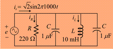
For the network in Fig. 16.82:
a. Calculate E, IR, and lL, in phasor form.
b. Calculate the total power factor, and indicate whether it is leading or lagging.
c. Calculate the average power delivered to the circuit.
d. Draw the admittance diagram.
e. Draw the phasor diagram of the currents Is. IR. and lL, and the voltage E.
f. Find the current lc for each capacitor using only Kirchhoff’s current law.
g. Find the series circuit of one resistive and reactive element that will have the same impedance as the original circuit.

Want to see the full answer?
Check out a sample textbook solution
Chapter 16 Solutions
Introductory Circuit Analysis; Laboratory Manual For Introductory Circuit Analysis Format: Kit/package/shrinkwrap
- 6.2 The triangular current pulse shown in Fig. P6.2 is applied to a 500 mH inductor.a) Write the expressions that describe i(t) in the four intervals t60, 0...t...25ms, 25 ms ... t ... 50 ms, and t 7 50 ms.b) Derive the expressions for the inductor volt- age, power, and energy. Use the passive sign convention.arrow_forwardOnly if you know what you are doing, you should attempt all this questions, don't use Artificial intelligence or it's screen shotarrow_forwardDon't use ai to answer I will report you answerarrow_forward
- 15) Complex numbers 21 and 22 are given by Δ Δ Δ Z₁ = 21-60° 22 = 5/45° Determine in polar form: Z, Z₂ b) 21/22 Z₁ C) Z, Z₂ dz 2 zz Z f) JZ ₂ 9) z, (z₂-z₁) * ~22/(Z1+Zz) FAAAAAA Aarrow_forwardform: Express The following Complex numbers in rectangular № 2, b) Z₂ = -3e-jπ/4 c) 23 = √ 3 e d 24 11 -j 25 = ==J 3 -4 2 -j3π/4 f) 26 = (2 + j) 9) 2₂ = (3-j2)³ g D 27 AAA D A 35arrow_forward0) Express The following complex numbers in polar form: az₁ = 3+ j4 2 b) 2₂ = -6+j8 C) 23 = 6j4 Z4=j2 d) 24 = j2 e) 25 = (2+ j)² 3 4) 26 = (3-j2) ³ JZ7 = (1+j) ½/2 27 D D D D D AA D AALarrow_forward
- 21) Determine. The phasor counterparts of the following sinusoidal functions: (a) V₁ (t) = 4 cos (377-30°) V (B) V₂ (t) = -2sin (8T x 10"+ + 18°) V e) V3 (t) = 3 sin (1000 + + 53°)-4c05 (1000 t -17°) v AAA AAAAAarrow_forwardI need help with this problem and an explanation of the solution for the image described below. (Introduction to Signals and Systems)arrow_forwardTutorial - Design of Common-Gate (CG) Amplifier Design a common-gate NMOS amplifier with the following parameters: Supply Voltage (VDD): 10 V ⚫Threshold Voltage (Vth): 2 V •Overdrive Voltage (Vov) = VGS-Vth: 1 V • Desired Voltage Gain Av: 10 V/V • Transconductance gm: to be determined •Ensure that the NMOS operates in the saturation region. ⚫ Design Vos to ensure saturation and enough voltage swing. C₁ Vin +VDD RD C₂ V out Rs WI RLarrow_forward
