
Videos
- (a) For the circuit in Fig. 14.97, draw the new circuit after it has been scaled by Km = 200 and Kf = 104.
- (b) Obtain the Thevenin equivalent impedance at terminals a-b of the scaled circuit at ω = 104 rad/s.
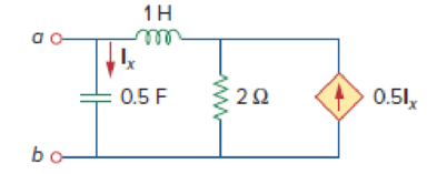
Figure 14.97
(a)
Draw the new circuit for the circuit in Figure 14.97 after it has been magnitude scaled by a factor of
Explanation of Solution
Given data:
Refer to Figure 14.97 in the textbook.
The value of the magnitude scaling factor
The value of the frequency scaling factor
Formula used:
Consider the equations used in magnitude and frequency scaling.
Write the expression to calculate the scaled resistor.
Here,
Write the expression to calculate the scaled inductor.
Here,
Write the expression to calculate the scaled capacitor.
Here,
Calculation:
The given circuit is redrawn as Figure 1.
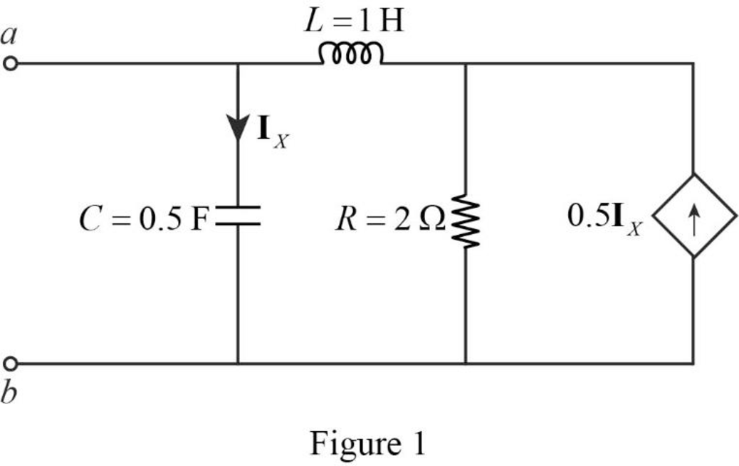
Refer to Figure 1, the value of the resistor
Substitute
Substitute
Substitute
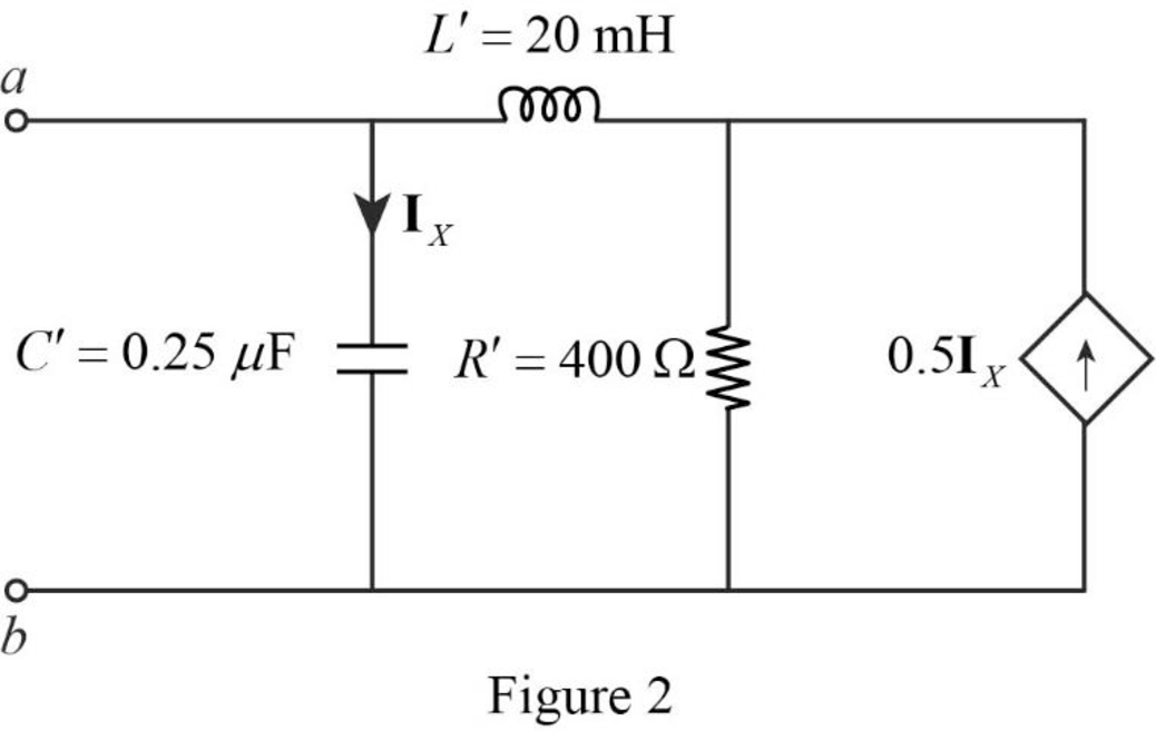
The redesigned circuit is drawn as Figure 2 which is obtained by using the magnitude and frequency scaling on the circuit in Figure 1.
Conclusion:
Thus, the new circuit for the circuit in Figure 14.97 is drawn by using the magnitude and frequency scaling.
(b)
Find the value of the Thevenin equivalent impedance at terminals a-b of the scaled circuit.
Answer to Problem 80P
The value of the Thevenin equivalent impedance
Explanation of Solution
Given data:
The value of the angular frequency
Formula used:
Write the expression to calculate the impedance of the passive elements resistor, inductor and capacitor in s-domain.
Here,
Calculation:
Use equation (4) to find
Use equation (5) to find
Use equation (6) to find
Insert a
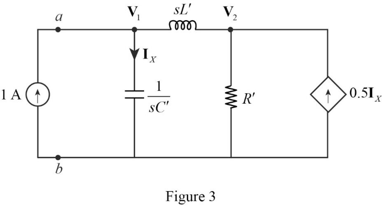
Apply Kirchhoff’s current law on Figure 3 to find
Rearrange the above equation.
Apply Kirchhoff’s current law on Figure 3 to find
Refer to Figure 3, the current
Substitute
By comparing the equations (7) and (9), the following equation is obtained.
Rearrange the above equation to find
Substitute
Simplify the above equation.
Simplify the above equation to find
Refer to Figure 3, the Thevenin equivalent impedance across the a-b terminals are calculated as follows.
Substitute
Substitute
Substitute
Simplify the above equation to find
Conclusion:
Thus, the value of the Thevenin equivalent impedance
Want to see more full solutions like this?
Chapter 14 Solutions
EE 98: Fundamentals of Electrical Circuits - With Connect Access


- 7.48 Determine the Thévenin equivalent of the circuit in Fig. P7.48 at terminals (a,b), given that Us(t) 12 cos 2500t V, = is(t)=0.5 cos (2500t - 30°) A.arrow_forwardPower system studies on an existing system have indicated that 2400 MW are to be transmitted for a distance of 400 Km. The voltage levels being considered include 345 kV, 500 kV, and 765 kV. For a preliminary design based on the practical line loadability, you may assume the following surge impedances 345 kV Zc=320 2 500 kV Zc=290 765 kV Zc=265 The line wavelength may be assumed to be 5000 km. The practical line loadability may be based on a load angle of 35º. Assume |Vs| = 1.0 pu and |Vr|=0.9 pu. a) Determine the number of three-phase transmission circuits required for each voltage level. Each transmission tower may have up to two circuits. To limit the corona loss, all 500-kV lines must have at least two conductors per phase, and all 765-kV lines must have at least four conductors per phase. b) The bundle spacing is 45 cm. The conductor size should be such that the line would be capable of carrying current corresponding to at least 5000 MVA. Determine the number of conductors in the…arrow_forwardGiven handwritten correct solution do not use AIarrow_forward
- 2. If the Ce value in Fig. 11-7 is changed to 0.1 μF, is the output still a PWM waveform? Explain. C₁ 0.014 C₂ 100 R₁ 300 HF 8 Vcc 4 reset output 3 discharge 7 2 trigger 5 control voltage U₁ LM555 6 threshold GND ODUCT R₂ 10k ww Bo +12 V 22 R3 1k VR 5k www Re 300 C5 100 ww 8 Vcc 4 reset output 3 2 trigger 7 discharge ли R7 10k PWM Output threshold C6 -0.014 5 control voltage GND Rs 2k CA U2 LM555 1 100μ C3 0.01 Audio lutput Fig. 11-7 Pulse width modulatorarrow_forwardPROD 1. What is the function of VR, in Figs. 11-2 and 11-7. DL RO 0.014 +12V R₁ 1k ww Vin(+) 6 C₁ 0.1μ Audio input HH VRI Vin(-) 4 U1 HА741 10k ww R2 10k UCTS 0.01 μ -12V PWM output Fig. 11-2 The pulse width modulator based on μA741 +12 V ° C₂ 100 R₁ 300 Re 300 Cs 100 ww ww Vcc 4 reset 2 trigger 5 control voltage U₁ LM555 GND www R₂ T₁ 10k output 3 discharge Z Voc output 3 reset VR₁ 5k 2 trigger 7 discharge Ra 1k threshold 6 control 6 threshold voltage GND Rs CA U2 LM555 1 2k 100 Ca 0.01 Audio lutput www R7 10k O PWM C6 -0.014 Fig. 11-7 Pulse width modulator 11/9 Outputarrow_forwardPRO3. In a point of view of voltage polarity, what is the difference between the output PWM signals in experiments 11-1 and 11-2? H ICTS Experiment 11-1.. Pulse Width Modulator Using uA741 Experiment 11-2 Pulse Width Modulator Using LM555arrow_forward
- 9.58 Using Fig. 9.65, design a problem to help other ed students better understand impedance combinations. Figure 8 65 ww C L R₁ www R2arrow_forwardindicate which of the following switches may be used to control the loads listedarrow_forwardEXAMPLE 3.15 Consider a sinusoidal signal g(t) = Acos (2лfot+), where the parameters A, fo, and are nonzero constants representing the amplitude, frequency, and initial phase of the sinusoidal signal, respectively. Determine if it is an energy signal or a power signal or neither.arrow_forward
 Introductory Circuit Analysis (13th Edition)Electrical EngineeringISBN:9780133923605Author:Robert L. BoylestadPublisher:PEARSON
 Delmar's Standard Textbook Of ElectricityElectrical EngineeringISBN:9781337900348Author:Stephen L. HermanPublisher:Cengage Learning
 Programmable Logic ControllersElectrical EngineeringISBN:9780073373843Author:Frank D. PetruzellaPublisher:McGraw-Hill Education
 Fundamentals of Electric CircuitsElectrical EngineeringISBN:9780078028229Author:Charles K Alexander, Matthew SadikuPublisher:McGraw-Hill Education
 Electric Circuits. (11th Edition)Electrical EngineeringISBN:9780134746968Author:James W. Nilsson, Susan RiedelPublisher:PEARSON
 Engineering ElectromagneticsElectrical EngineeringISBN:9780078028151Author:Hayt, William H. (william Hart), Jr, BUCK, John A.Publisher:Mcgraw-hill Education,