Videos
Find the bandwidth and center frequency of the band-stop filter of Fig. 14.89.
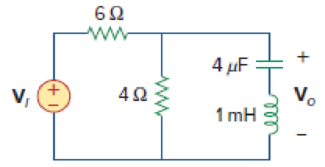
Figure 14.89
Find the bandwidth and center frequency of the band-stop filter shown in Figure 14.89.
Answer to Problem 59P
The value of the bandwidth
Explanation of Solution
Given data:
Refer to Figure 14.89 in the textbook.
Formula used:
Write the expression to calculate the impedance of the passive elements resistor, inductor and capacitor in s-domain.
Here,
Calculation:
The given circuit is drawn as Figure 1.
Use equation (1) to find
Use equation (1) to find
Use equation (2) to find
Use equation (3) to find
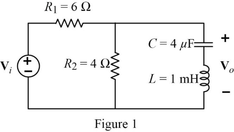
The s-domain circuit of the Figure 1 is drawn as Figure 2.
Write the general expression to calculate the transfer function of the circuit in Figure 2.
Here,
Refer to Figure 2, the series connected impedances
Therefore, the equivalent impedance is calculated as follows.
Simplify the above equation to find
The reduced circuit of Figure 2 is drawn as Figure 3.
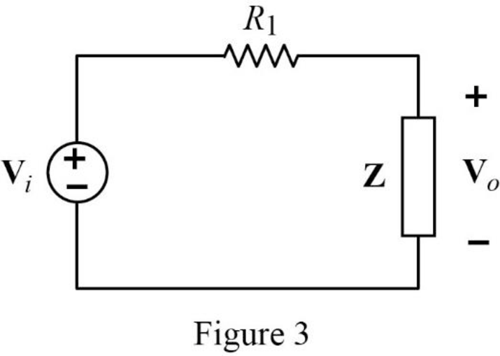
Apply voltage division rule on Figure 3 to find
Rearrange the above equation to find
Substitute
Substitute
Refer to Figure 3, the input impedance is expressed as,
Substitute
Substitute
Simplify the above equation to find
At resonance condition, the imaginary part of the impedance should be equal to zero. Therefore, equate the imaginary part of the above equation to zero.
Simplify the above equation to find
Take square root on both sides of the above equation to find
Substitute
Simplify the above equation to find
Substitute
Substitute
Substitute
Simplify the above equation to find
At corner frequency
Substitute
Simplify the above equation.
Substitute
Simplify the above equation.
Square on both sides of the above equation to simplify it.
Simplify the above equation.
Simplify the above equation.
Assume
Write a general expression to calculate the roots of quadratic equation
Compare the equation (8) with the quadratic equation
Substitute
Substitute the roots of characteristic equation in equation (8).
Substitute
Simplify the equation (10) to find
Take square root on both sides of the above equation to find
Simplify the equation (10) to find
Take square root on both sides of the above equation to find
Write the expression to calculate the bandwidth of the band-stop filter.
Here,
Substitute
Conclusion:
Thus, the value of the bandwidth
Want to see more full solutions like this?
Chapter 14 Solutions
EBK FUNDAMENTALS OF ELECTRIC CIRCUITS
Additional Engineering Textbook Solutions
Vector Mechanics for Engineers: Statics and Dynamics
Mechanics of Materials (10th Edition)
Modern Database Management
SURVEY OF OPERATING SYSTEMS
Vector Mechanics For Engineers
Electric Circuits. (11th Edition)


- Medium 1 is a lossless dielectric (ε₁=ε,ε, μ₁=μ₁, σ₁=0) Medium 2 is a lossless dielectric (ε=&&₂, μ=μ₁, σ₁=0) [бг Мо о = = 0] [2 Mo σ₂ = 0] E₁ (z) = Ele² + Пe+jB₁²] E2 (z) = E Te² and tot = constant 1. For the case εr1 = 1, &r2= 16, E₁x=1 V/m and a frequency f = 750 MHz determine: λι = n₁ = 22 = n2= r = T= 2. The magnitude |E1 tot (z)| will show an interference pattern in region 1 as: E˜(z)=E,{1+Te®®]e¯MS =E||{1+Te^^^^\]e=##} | = |E|+Texp(j) For an incident field E₁x=1 V/m SKETCH the magnitude of E1 tot (z)| and |E20 (z) on the graph below. Plot the values at 2/4 increments and sketch between. What is the SWR?arrow_forwardPlease don't use AIarrow_forwardPlease don't use AIarrow_forward
- 3) In the ideal autotransformer circuit shown below find 11, 12 and lo. Find the average power delivered to the load. (hint: write KVL for both sides) 20/30° V(+ 2-1602 200 turns V₂ 10 + j40 Ω 80 turns V₁arrow_forward11-2) Now consider that white noise (i.e., noise with a PSD that is constant with frequency) is introduced in the channel of the system described in the previous problem. An ideal low pass filter is used at the receiver input to reduce the noise as much as possible, while transmitting the desired signal. (a) By what factor should the cutoff frequency of the noise reduction filter be reduced in the 16-PAM case, compared to binary? (b) By what factor will the noise power at the decision circuit be reduced in the 16-PAM case? (c) By what factor will the noise amplitude at the decision circuit be reduced in the 16-PAM case? (d) To obtain the same symbol error rate for 16-PAM as for binary, how should the minimum level spacing for 16-PAM compare to binary? (e) If the 16-PAM level spacing is adjusted according to part (d) above, by what factor will the average signal power be increased in the 16-PAM case, compared to binary?arrow_forward11-1) similar to Lathi & Ding, Prob. P.6.7-5 Data at a bit rate Rb must be transmitted using either binary NRZ polar signaling or 16-ary PAM NRZ polar signaling. (a) By what factor will the symbol rate be reduced in the 16-PAM case? (b) By what factor will bandwidth required from the (lowpass) channel be reduced in the 16-PAM case? (c) Assuming the minimum spacing between pulse levels must be the same in both cases, by what factor will the average power be increased in the 16-PAM case? [Hint: take the pulse amplitudes to be ±A in the binary case, and ±A, ±3A, ±5A,..., ±154, and recall that scaling pulse amplitude by a factor k scales the pulse energy by a factor R². Assume that the data is random, so that all 16 levels are equally likely, and that the same pulse shape is used in both cases.] Warning: Solutions to the textbook problem that are posted online are mostly wrong. Work it out for yourself.arrow_forward
- 11-3) similar to Lathi & Ding, Prob. P.6.8-1 Consider the carrier modulator shown in the figure below, which transmits a binary carrier signal. The baseband generator uses polar NRZ signaling with rectangular pulses. The data rate is 8 Mbit/s. (a) If the modulator generates a binary PSK signal, what is the bandwidth of the modulated output? (b) If the modulator generates FSK with the difference fel - fco = 6 MHz (cf. Fig 6.32c), determine the modulated signal bandwidth. Binary data source Baseband signal generator Modulated output Modulator N-E---arrow_forwardFor the circuit shown, find (i) closed-loop voltage gain (ii) Z i of the circuit (iii) f_max. The slew rate is 0.6V/us. ((write your answer in Kilo ohm)) 2Vpp R ww 20 kQ R₁ ww 200 ΚΩ 9+18 V - 18 V 10 kn R₁₂ ΚΩ ((write your answer in KHz))arrow_forwardillustrate the phenomenon of phase reversal in CE amplifier i- When signal current =OA, so IB-8uA ii- When input signal reaches positive peak, so IB=16uA ii- When input signal reaches negative peak, so IB=4uA R₁ www + Vcc = 12V Rc=6kn 16 A 8 μA 4 μА 0 www RE ẞ = 100 VCarrow_forward
- In the circuit shown, find the voltage gain. Given that ẞ = 80 and input resistance Rin=2kQ. SIGNAL +10 V Rc=6kn 4-2 210arrow_forwardFor the transistor amplifier shown, R₁-11kQ, R2=6kQ, Rc=2kQ, RE-3kQ and R₁=2k0. (i) Draw d.c. load line (ii) Determine the DC operating point (iii) Draw a.c. load line. Assume V_BE = 0.7 V. and determine the new operating point + Vcc = 15 V RC Cc Cin R1 wwwwww wwwww R₁₂ RE CE RLarrow_forwardthe first part is the second part write your answer such as: (AND, OR, INVERTER, NAND, NOR) D₁ AK D, R₁ B K First Part? the third part is , and the total are R4 R7 Output R5 R₁ T R6 R3 -UBB Second Part? Third Part? Total?arrow_forward
 Introductory Circuit Analysis (13th Edition)Electrical EngineeringISBN:9780133923605Author:Robert L. BoylestadPublisher:PEARSON
 Delmar's Standard Textbook Of ElectricityElectrical EngineeringISBN:9781337900348Author:Stephen L. HermanPublisher:Cengage Learning
 Programmable Logic ControllersElectrical EngineeringISBN:9780073373843Author:Frank D. PetruzellaPublisher:McGraw-Hill Education
 Fundamentals of Electric CircuitsElectrical EngineeringISBN:9780078028229Author:Charles K Alexander, Matthew SadikuPublisher:McGraw-Hill Education
 Electric Circuits. (11th Edition)Electrical EngineeringISBN:9780134746968Author:James W. Nilsson, Susan RiedelPublisher:PEARSON
 Engineering ElectromagneticsElectrical EngineeringISBN:9780078028151Author:Hayt, William H. (william Hart), Jr, BUCK, John A.Publisher:Mcgraw-hill Education,