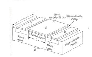
Refer to the generic FET figure for this problem. And select the correct answer inside of the parenthesis (a) If the substrate doping is NA = 5 x 1016 cm-3, the basic structure is (CMOS, PMOS, NMOS, JFET, MESFET) and the inverted channel charge carriers are (HOLES, ELECTRONS, BOTH HOLES AND ELECTRONS, NEUTRONS, PHOTONS). (b) IF the subbstrate doping is changed to be ND = 5 x 1016 cm- 3, the basic structure is (CMOS, PMOS, NMOS, JFET, MESFET) and the inverted channel charge carriers are (HOLES, ELECTRONS, BOTH HOLES AND ELECTRONS, NEUTRONS, PHOTONS) (c) Assume L = 50 nm, W = 500 nm, tox = 200 Å. Units are important!!!!!! Compute Cox and Compute CTotal


Refer to the generic FET figure for this problem. And select the correct answer inside of the parenthesis
(a) If the substrate doping is NA = 5 x 1016 cm-3, the basic
structure is (CMOS, PMOS, NMOS, JFET, MESFET) and the inverted
channel charge carriers are (HOLES, ELECTRONS, BOTH HOLES
AND ELECTRONS, NEUTRONS, PHOTONS).
(b) IF the subbstrate doping is changed to be ND = 5 x 1016 cm-
3, the basic structure is (CMOS, PMOS, NMOS, JFET, MESFET) and
the inverted channel charge carriers are (HOLES, ELECTRONS, BOTH
HOLES AND ELECTRONS, NEUTRONS, PHOTONS)
(c) Assume L = 50 nm, W = 500 nm, tox = 200 Å. Units are important!!!!!!
Compute Cox and Compute CTotal

Given the generic figure of FET:
a) If the substrate doping is NA = 5 x 1016 cm-3, then we need to find what is the basic structure out of the options( (CMOS, PMOS, NMOS, JFET, MESFET) and also we need to find the inverted channel charge carrier out of the options(HOLES, ELECTRONS, BOTH HOLES AND ELECTRONS, NEUTRONS, PHOTONS).
b) If the substrate doping is changed to be ND = 5 x 1016 cm-3, then we need to find what is the basic structure out of the options( (CMOS, PMOS, NMOS, JFET, MESFET) and also we need to find the inverted channel charge carrier out of the options(HOLES, ELECTRONS, BOTH HOLES AND ELECTRONS, NEUTRONS, PHOTONS).
c) Assuming L = 50 nm, W = 500 nm, tox = 200 Å. We need to compute Cox and CTotal.

Step by step
Solved in 4 steps with 2 images


