FET Pot-Pourri. Refer to the generic FET figure for this problem. If the substrate doping is N = 5 x 1016 cm³, the basic structure is (CMOS, PMOS, NMOS, JFET, MESFET) and the inverted channel charge carriers are (HOLES, ELECTRONS, BOTH HOLES AND ELECTRONS, NEUTRONS, PHOTONS). Metal Silicon dioxide (SIO2) (or polysilicon) S G Channel region p-type substrate (body) Source (b) If the substrate doping is changed to be N, = 5 x 10“ cm³, region Drain region the basic structure is (CMOS, PMOS, NMOS, JFET, MESFET) and the inverted channel charge carriers are (HOLES, В ELECTRONS, BOTH HOLES AND ELECTRONS, NEUTRONS, PHOTONS) Assume L= 50 nm, W = 500 nm, t = 200 Ă. Units are important!!!!!! %3D c) Compute Cox Compute CTotal


Given the internal structure of FET:
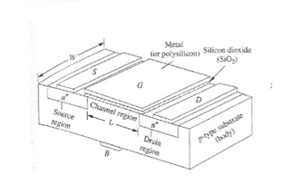
a) If the substrate doping is NA = 5 x 1016 cm-3, then we need to find what is the basic structure out of the options( (CMOS, PMOS, NMOS, JFET, MESFET) and also we need to find the inverted channel charge carrier out of the options(HOLES, ELECTRONS, BOTH HOLES AND ELECTRONS, NEUTRONS, PHOTONS).
b) If the substrate doping is changed to be ND = 5 x 1016 cm-3, then we need to find what is the basic structure out of the options( (CMOS, PMOS, NMOS, JFET, MESFET) and also we need to find the inverted channel charge carrier out of the options(HOLES, ELECTRONS, BOTH HOLES AND ELECTRONS, NEUTRONS, PHOTONS).
c) Assuming L = 50 nm, W = 500 nm, tox = 200 Å. We need to compute Cox and CTotal.

Step by step
Solved in 4 steps with 2 images


