Concept explainers
Videos
The unknown parameters using Kirchhoff’s Laws.
Answer to Problem 3PP
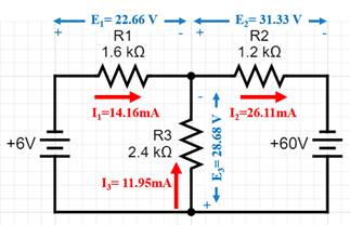
| ES1=6 V | E1= 0.89 V | E2= 20.89 V | E3= 11.1 V |
| ES2=60 V | I1= 1.31 mA | I2= 20.89 mA | I3= 22.2 mA |
| R1=1.6kΩ | R2= 1.2 kΩ | R3= 2.4 kΩ |
Explanation of Solution
We will use Kirchhoff’s Voltage law to solve for the unknown parameters.
Consider two loops LOOP 1 and LOOP 2 with their respective loop currents I1 and I2
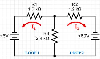
Using KVL in loop 1,
Using KVL in loop 2,
From equation (1), we can write I2as ,
Substitute this expression for I2in equation (2),
The negative sign indicates that the direction of current is different from that assumed at the start.
Substitute the value of I1 in equation (3).
CurrentI3 is the sum of currents I1 and I2
The voltage drops are obtained by using Ohm’s Law,
The results are summarized in the figure below,
Want to see more full solutions like this?
Chapter 9 Solutions
Mindtap Electrical, 4 Terms (24 Months) Printed Access Card For Herman's Delmar's Standard Textbook Of Electricity, 6th (mindtap Course List)


- 4. Please find the stability margins from the following Bode diagrams. Bode Diagram Phase (deg) Magnitude (dB) 50 -100 -90 -135 -180 -270 10" 10° Frequency (rad/sec) 10'arrow_forward2. Please use asymptotes to draw the Bode diagrams of the following transfer function. Please label the axes to show the cut-off frequencies and key values on vertical axes and label each asymptote with its slope. G(s) s+10 s(s²+10s+100)arrow_forwardFind Voarrow_forward
- J. na ul-n-1) X (n) = na^ = na^ u(-(n+1)) (1-1+4)= 741-1 4[cn+1)] +1 * Z (^- 1-1 (n-1) a て why ✓ (n) Z , ༥(-༡) ur-n) Znxcm) -Zx X (n) (n-1) a auc-n) = X(n) ぞ 2-9³arrow_forwardTurn trip logic into boolean algebra gates logic?arrow_forwardFind the Z-transform including the region of convergence for the following function 12 (¹)" [u(n) – u(n − 5)] -arrow_forward
- Find the inverse Z-traform of X(z)= z 2 +z (z-0.125)³ (z-0.25)arrow_forwardA separately excited 6-kilowatt generator has a terminal voltage of 135V at no load. At full load, the terminal voltage is 120V with speed and field excitation unchanged. Armature resistance = = 0.25 ohm. A. What is the amount of voltage decrease caused by armature reaction and the voltage regulation?arrow_forwardJ. A sampling system can be set to adjust its sampling rate in 25 He steps. Considering the signal spectra pleted below, specify the minimum sampling rate setting for the signals: a)x(1) b)(1)+(1) 985)+20 0,09 0:00 0,0 106) 100) SORO -2501 250V (1500+501) 。 1500+50V 201 2500arrow_forward
 EBK ELECTRICAL WIRING RESIDENTIALElectrical EngineeringISBN:9781337516549Author:SimmonsPublisher:CENGAGE LEARNING - CONSIGNMENT
 Electricity for Refrigeration, Heating, and Air C...Mechanical EngineeringISBN:9781337399128Author:Russell E. SmithPublisher:Cengage Learning