
Concept explainers
The unknown parameters using Kirchhoff’s Laws.
Answer to Problem 1PP
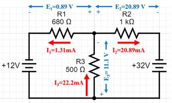
| ES1= 12 V | E1= 0.89 V | E2= 20.89 V | E3= 11.1 V |
| ES2= 32 V | I1= 1.31 mA | I2= 20.89 mA | I3= 22.2 mA |
| R1= 680 Ω | R2=1000 Ω | R3=500 Ω |
Explanation of Solution
We will use Kirchhoff’s Voltage law to solve for the unknown parameters.
Consider two loops LOOP 1 and LOOP 2 with their respective loop currents I1 and I2
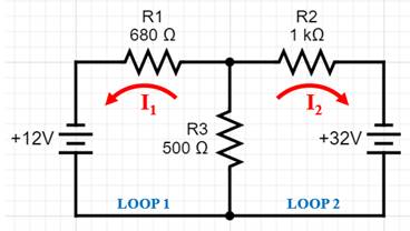
Using KVL in loop 1,
Using KVL in loop 2,
From equation (1), we can write I2as ,
Substitute this expression for I2in equation (2),
Substitute the value of I1 in equation (3).
CurrentI3 is the sum of currents I1 and I2
The voltage drops are obtained by using Ohm’s Law,
The results are summarized in the figure below,
Want to see more full solutions like this?
Chapter 9 Solutions
DELMAR'S STANDARD TEXT OF ELECTRICITY


- Don't use ai to answer I will report you answerarrow_forward3) Find the valve of V using the Thevenin Equivalent Circuit and then determine if the 8 ohm resistor allows maximum power transfer. If not, then what value should the 8 ohm resist or be changed to for maximum power transfer? ZA 360 Am 6t + 22V V 3402 22 62 Mw marrow_forwardFind the valve of the voltage Vx using the THEVENIN 2) equivalent circuit and redo the problem with the NORTON equivalent circuit. Show both the flavinen and Norton Circuits DAY ww 1 23 www + 4444 5 63arrow_forward
- Figure shows the block diagram of a feedback control system with a disturbance signal N(s). Obtain the output Y(s) due to both R(s) and N(s).arrow_forwardA 3-phase, 6-pole induction motor is con- nected to a 60 Hz supply. The voltage in- duced in the rotor bars is 4 V when the ro- tor is locked. If the motor turns in the same direction as the flux, calculate the approxi- mate voltage induced and its frequency: a. At 300 r/min b. At 1000 r/min c. At 1500 r/minarrow_forwardMake a drawing of the magnetic field cre- ated by a 3-phase, 12-pole induction motor. How can we change the direction of rota- tion of a 3-phase induction motor?arrow_forward
- Describe the principle of operation of a lin- ear induction motor.arrow_forwardName the principal components of an in- duction motor. Explain how a revolving field is set up in a 3-phase induction motor.arrow_forwardAnswer all the questions (a) How much power is the wind farm generating? (b) How much power is the solar farm generating? (c) Find the power delivered to the AC motor. (d) If the AC motor requires at least 45 kW of power, is the system able to provide that power? If not, how many additional series PV modules should be added to each string (we want to keep the same number of modules in each string)? If so, how many modules can be removed from each string while still meeting the requirements?arrow_forward
- An open-circuit voltage of 240 V appears across the slip-rings of a wound-rotor in- duction motor when the rotor is locked. The stator has 6 poles and is excited by a 60 Hz source. If the rotor is driven by a variable-speed dc motor, calculate the open-circuit voltage and frequency across the slip-rings if the dc motor turns a. At 600 r/min, in the same direction as the rotating field b. At 900 r/min, in the same direction as the rotating field c. At 3600 r/min, opposite to the rotating fieldarrow_forwardIf we double the number of poles on the stator of an induction motor, will its syn- chronous speed also double? The rotor of an induction should never be locked while full voltage is being applied to the stator. Explain. Why does the rotor of an induction motor turn slower than the revolving field?arrow_forwarda. Calculate the synchronous speed of a 3-phase, 12-pole induction motor that is excited by a 60 Hz source. b. What is the nominal speed if the slip at full-load is 6 percent?arrow_forward
 EBK ELECTRICAL WIRING RESIDENTIALElectrical EngineeringISBN:9781337516549Author:SimmonsPublisher:CENGAGE LEARNING - CONSIGNMENT
 Electricity for Refrigeration, Heating, and Air C...Mechanical EngineeringISBN:9781337399128Author:Russell E. SmithPublisher:Cengage Learning
 Power System Analysis and Design (MindTap Course ...Electrical EngineeringISBN:9781305632134Author:J. Duncan Glover, Thomas Overbye, Mulukutla S. SarmaPublisher:Cengage Learning