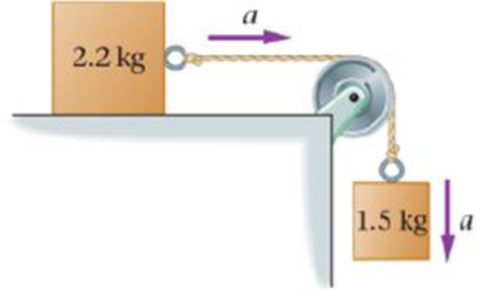
Predict/Calculate The blocks in Figure 6-69 have an acceleration of magnitude a = 1.1 m/s 2 . (a) Is the tension in the string greater than, less than, or equal to (1.5 kg) × 9.81 m/s 2 )? Explain. (b) What is the tension in the string connecting the blocks? (c) What is the magnitude of the force of kinetic friction acting on the upper block? (d) What is the coefficient of kinetic friction between the upper block and the horizontal surface?
Predict/Calculate The blocks in Figure 6-69 have an acceleration of magnitude a = 1.1 m/s 2 . (a) Is the tension in the string greater than, less than, or equal to (1.5 kg) × 9.81 m/s 2 )? Explain. (b) What is the tension in the string connecting the blocks? (c) What is the magnitude of the force of kinetic friction acting on the upper block? (d) What is the coefficient of kinetic friction between the upper block and the horizontal surface?
Predict/Calculate The blocks in Figure 6-69 have an acceleration of magnitude a = 1.1 m/s2. (a) Is the tension in the string greater than, less than, or equal to (1.5 kg) × 9.81 m/s2)? Explain. (b) What is the tension in the string connecting the blocks? (c) What is the magnitude of the force of kinetic friction acting on the upper block? (d) What is the coefficient of kinetic friction between the upper block and the horizontal surface?
Definition Definition Force that opposes motion when the surface of one item rubs against the surface of another. The unit of force of friction is same as the unit of force.
How can you tell which vowel is being produced here ( “ee,” “ah,” or “oo”)? Also, how would you be able to tell for the other vowels?
You want to fabricate a soft microfluidic chip like the one below. How would you go about
fabricating this chip knowing that you are targeting a channel with a square cross-sectional
profile of 200 μm by 200 μm. What materials and steps would you use and why? Disregard the
process to form the inlet and outlet.
Square Cross Section
1. What are the key steps involved in the fabrication of a semiconductor device.
2. You are hired by a chip manufacturing company, and you are asked to prepare a silicon wafer
with the pattern below. Describe the process you would use.
High Aspect
Ratio
Trenches
Undoped Si Wafer
P-doped Si
3. You would like to deposit material within a high aspect ratio trench. What approach would you
use and why?
4. A person is setting up a small clean room space to carry out an outreach activity to educate high
school students about patterning using photolithography. They obtained a positive photoresist, a
used spin coater, a high energy light lamp for exposure and ordered a plastic transparency mask
with a pattern on it to reduce cost. Upon trying this set up multiple times they find that the full
resist gets developed, and they are unable to transfer the pattern onto the resist. Help them
troubleshoot and find out why pattern of transfer has not been successful.
5. You are given a composite…
Physics for Scientists and Engineers: A Strategic Approach, Vol. 1 (Chs 1-21) (4th Edition)
Knowledge Booster
Learn more about
Need a deep-dive on the concept behind this application? Look no further. Learn more about this topic, physics and related others by exploring similar questions and additional content below.


 Classical Dynamics of Particles and SystemsPhysicsISBN:9780534408961Author:Stephen T. Thornton, Jerry B. MarionPublisher:Cengage Learning
 Physics for Scientists and Engineers: Foundations...PhysicsISBN:9781133939146Author:Katz, Debora M.Publisher:Cengage Learning
 Principles of Physics: A Calculus-Based TextPhysicsISBN:9781133104261Author:Raymond A. Serway, John W. JewettPublisher:Cengage Learning
 Physics for Scientists and Engineers, Technology ...PhysicsISBN:9781305116399Author:Raymond A. Serway, John W. JewettPublisher:Cengage Learning
 Glencoe Physics: Principles and Problems, Student...PhysicsISBN:9780078807213Author:Paul W. ZitzewitzPublisher:Glencoe/McGraw-Hill
 College PhysicsPhysicsISBN:9781285737027Author:Raymond A. Serway, Chris VuillePublisher:Cengage Learning