
EBK THE ANALYSIS AND DESIGN OF LINEAR C
8th Edition
ISBN: 9781119228226
Author: Toussaint
Publisher: YUZU
expand_more
expand_more
format_list_bulleted
Concept explainers
Videos
Textbook Question
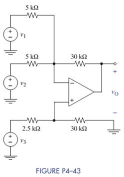
Chapter 4, Problem 4.43P
Find
Expert Solution & Answer
Want to see the full answer?
Check out a sample textbook solution
Students have asked these similar questions
For a band-rejection filter, the response drops below this half power point at two locations as visualised in Figure 7, we need to find these
frequencies. Let's call the lower frequency-3dB point as fr and the higher frequency -3dB point fH. We can then find out the bandwidth as
f=fHfL, as illustrated in Figure 7.
0dB
Af
-3 dB
Figure 7. Band reject filter response diagram
Considering your AC simulation frequency response and referring to Figure 7, measure the following from your AC simulation. 1% accuracy:
(a) Upper-3db Frequency (fH) =
Hz
(b) Lower-3db Frequency (fL) =
Hz
(c) Bandwidth (Aƒ) =
Hz
(d) Quality Factor (Q) =
P 4.4-21 Determine the values of the node voltages V1, V2, and
v3 for the circuit shown in Figure P 4.4-21.
29
ww
12 V
+51
Aia
ww
22.
+21
ΖΩ
www
ΖΩ
w
+371
①1
1 A
1. What is the theoretical attenuation of the output voltage at the resonant frequency? Answer to within 1%, or enter 0, or infinity (as “inf”)
Attenuation =
Chapter 4 Solutions
EBK THE ANALYSIS AND DESIGN OF LINEAR C
Ch. 4 - Find the voltage gain vO/vS and current gain iO/ix...Ch. 4 - Prob. 4.2PCh. 4 - Prob. 4.3PCh. 4 - Prob. 4.4PCh. 4 - Find the voltage gain vO/vS in Figure P4-5.Ch. 4 - Find the voltage gain vO/vS in Figure P4-6.Ch. 4 - Find an expression for the current gain iO/iS in...Ch. 4 - Prob. 4.8PCh. 4 - Prob. 4.9PCh. 4 - Find an expression for the voltage gain vO/vs in...
Ch. 4 - Prob. 4.12PCh. 4 - In the circuit of Figure P4-13, the VCVS has of...Ch. 4 - Prob. 4.14PCh. 4 - (a) Find the Thévenin equivalent circuit that the...Ch. 4 - Prob. 4.16PCh. 4 - Prob. 4.18PCh. 4 - Prob. 4.19PCh. 4 - The circuit parameters in figure P4-21 are...Ch. 4 - The circuit parameters in Figure P4-21 are...Ch. 4 - The parameters of the transistor in Figure P4-23...Ch. 4 - Prob. 4.25PCh. 4 - Find the voltage gain of each OP AMP circuit shown...Ch. 4 - Considering simplicity and standard 10 tolerance...Ch. 4 - Two OP AMP circuits are shown in Figure P4-28....Ch. 4 - Prob. 4.29PCh. 4 - What is the range of the gain vO/vS in Figure...Ch. 4 - Using only one OP AMP, design a circuit that...Ch. 4 - Design a circuit using only one OP AMP that...Ch. 4 - Prob. 4.36PCh. 4 - For the circuit in Figure P4-37: (a) Find vO in...Ch. 4 - A young designer needed to amplify a 2-V signal by...Ch. 4 - Design two circuits to produce the following...Ch. 4 - Design a noninverting summer for five inputs with...Ch. 4 - For the circuit in Figure P4-41: Find vO in terms...Ch. 4 - The input-output relationship for a three-input...Ch. 4 - Find vo in terms of the inputs v1,v2, and v3 in...Ch. 4 - Prob. 4.44PCh. 4 - Prob. 4.45PCh. 4 - Prob. 4.46PCh. 4 - Prob. 4.47PCh. 4 - It is claimed that vO=vS when the switch is closed...Ch. 4 - Prob. 4.49PCh. 4 - Prob. 4.50PCh. 4 - Use node-voltage analysis in Figure P4-51 to show...Ch. 4 - Prob. 4.52PCh. 4 - Prob. 4.53PCh. 4 - For the block diagram of Figure P4-54: Find an...Ch. 4 - For the block diagram of Figure P4-55: Find an...Ch. 4 - For the circuit in Figure P4-56: Find vO in terms...Ch. 4 - Prob. 4.57PCh. 4 - Onan exam, students were asked to design an...Ch. 4 - Prob. 4.59PCh. 4 - For the circuit of Figure P4-60: Use node-voltage...Ch. 4 - Prob. 4.61PCh. 4 - Design a single OP AMP amplifier with a voltage...Ch. 4 - Design an OP AMP amplifier with a voltage gain of...Ch. 4 - Using a single OP AMP, design a circuit with...Ch. 4 - Design a differential amplifier with inputs v1 and...Ch. 4 - Using no more than two OP AMPs, design an OP AMP...Ch. 4 - Design a two-input noninverting summer that will...Ch. 4 - Design a three-input noninverting summer that will...Ch. 4 - Design a cascaded OP AMP circuit that will produce...Ch. 4 - Design a cascaded OP AMP circuit that will produce...Ch. 4 - Using the instrumentation amplifier shown in...Ch. 4 - Prob. 4.73PCh. 4 - Design a circuit that can produce vO=2000vTR2.6V...Ch. 4 - A requirement exists for an OP AMP circuit with...Ch. 4 - A requirement exists for an OP AMP circuit to...Ch. 4 - A particular application requires that an...Ch. 4 - Prob. 4.78PCh. 4 - The full-scale output of a six-bit DAC is 10.0 V....Ch. 4 - An R2R DAC is shown in Figure P4-80. The digital...Ch. 4 - A fifth bit is added to the R-2R DAC shown in...Ch. 4 - Prob. 4.82PCh. 4 - Prob. 4.83PCh. 4 - A small pressure transducer has the...Ch. 4 - A medical grade pressure transducer has been...Ch. 4 - The acid/alkaline balance of a fluid is measured...Ch. 4 - A photoresistor varies from 10 in bright sunlight...Ch. 4 - Your engineering firm needs an instrumentation...Ch. 4 - Prob. 4.90PCh. 4 - Prob. 4.92PCh. 4 - Prob. 4.93PCh. 4 - A five-bit flash ADC in Figure P4-94 uses a...Ch. 4 - Bipolar Power Supply Voltages The circuit in...Ch. 4 - Thermometer Design Problem There is a need to...Ch. 4 - High Bias Design Problem A particular pressure...Ch. 4 - Prob. 4.99IPCh. 4 - OP AMP Circuit Analysis and Design Find the...Ch. 4 - Instrumentation Amplifier with Alarm Strain gauges...
Knowledge Booster


Learn more about
Need a deep-dive on the concept behind this application? Look no further. Learn more about this topic, electrical-engineering and related others by exploring similar questions and additional content below.Similar questions
- What is the settling time for your output signal (BRF_OUT)? For this question, We define the settling time as the period of time it has taken for the output to settle into a steady state - ie when your oscillation first decays (aka reduces) to less than approximately 1/20 (5%) of the initial value. (a) Settling time = 22 μs Your last answer was interpreted as follows: Incorrect answer. Check 22 222 What is the peak to peak output voltage (BRF_OUT pp) at the steady state condition? You may need to use the zoom function to perform this calculation. Select a time point that is two times the settling time you answered in the question above. Answer to within 10% accuracy. (a) BRF_OUT pp= mVpp As you may have noticed, the output voltage amplitude is a tiny fraction of the input voltage, i.e. it has been significantly attenuated. Calculate the attenuation (decibels = dB) in the output signal as compared to the input based on the formula given below. Answer to within 1% accuracy.…arrow_forwardmy previous answers for a,b,d were wrong a = 1050 b = 950 d=9.99 c was the only correct value i got previously c = 100hz is correctarrow_forwardV₁(t) ww ZRI ZLI ZL2 ZTH Zci VTH Zc21 Figure 8. Circuit diagram showing calculation approach for VTH and Z TH we want to create a blackbox for the red region, we want to use the same input signal conditions as previously the design of your interference ector circuit: Sine wave with a 1 Vpp, with a frequency of 100 kHz (interference) Square wave with 2.4Vpp, with a frequency of 10 kHz (signal) member an AC Thevenin equivalent is only valid at one frequency. We have chosen to calculate the Thevenin equivalent circuit (and therefore the ackbox) at the interference frequency (i.e. 100 kHz), and the signal frequency (i.e. 10 kHz) as these are the key frequencies to analyse. Your boss is assured you that the waveform converter module has been pre-optimised to the DAB Receiver if you use the recommended circuit topology.arrow_forward
- Vs(t) + v(t) + vi(t) ZR ZL Figure 1: Second order RLC circuit Zc + ve(t) You are requested to design the circuit shown in Figure 1. The circuit is assumed to be operating at its resonant frequency when it is fed by a sinusoidal voltage source Vs (t) = 2sin(le6t). To help design your circuit you have been given the value of inductive reactance ZL = j1000. Assume that the amplitude of the current at resonance is Is (t) = 2 mA. Based on this information, answer the following to help design your circuit. Use cartesian notation for your answers, where required.arrow_forwardWhat is the attenuation at the resonant frequency? You should use the LTSpice cursors for your measurement. Answer to within 1% accuracy, or enter 0, or infinity (as "inf") (a) Attenuation (dB) = dB Check You may have noticed that it was significantly easier to use frequency-domain "AC" simulation to measure the attenuation, compared to the steps we performed in the last few questions. (i.e. via a time-domain "transient" simulation). AC analysis allows us to observe and quantify large scale positive or negative changes in a signal of interest across a wide range of different frequencies. From the response you will notice that only frequencies that are relatively close to 100 kHz have been attenuated. This is the result of the Band-reject filter you have designed, and shows the 'rejection' (aka attenuation) of any frequencies that lie in a given band. The obvious follow-up question is how do we define this band? We use a quantity known as the bandwidth. A commonly used measurement for…arrow_forwardV₁(t) ww ZRI ZLI ZL2 ZTH Zci VTH Zc21 Figure 8. Circuit diagram showing calculation approach for VTH and Z TH we want to create a blackbox for the red region, we want to use the same input signal conditions as previously the design of your interference ector circuit: Sine wave with a 1 Vpp, with a frequency of 100 kHz (interference) Square wave with 2.4Vpp, with a frequency of 10 kHz (signal) member an AC Thevenin equivalent is only valid at one frequency. We have chosen to calculate the Thevenin equivalent circuit (and therefore the ackbox) at the interference frequency (i.e. 100 kHz), and the signal frequency (i.e. 10 kHz) as these are the key frequencies to analyse. Your boss is assured you that the waveform converter module has been pre-optimised to the DAB Receiver if you use the recommended circuit topology.arrow_forward
- Vs(t) + v(t) + vi(t) ZR ZL Figure 1: Second order RLC circuit Zc + ve(t) You are requested to design the circuit shown in Figure 1. The circuit is assumed to be operating at its resonant frequency when it is fed by a sinusoidal voltage source Vs (t) = 2sin(le6t). To help design your circuit you have been given the value of inductive reactance ZL = j1000. Assume that the amplitude of the current at resonance is Is (t) = 2 mA. Based on this information, answer the following to help design your circuit. Use cartesian notation for your answers, where required.arrow_forwardFor a band-rejection filter, the response drops below this half power point at two locations as visualised in Figure 7, we need to find these frequencies. Let's call the lower frequency-3dB point as fr and the higher frequency -3dB point fH. We can then find out the bandwidth as f=fHfL, as illustrated in Figure 7. 0dB Af -3 dB Figure 7. Band reject filter response diagram Considering your AC simulation frequency response and referring to Figure 7, measure the following from your AC simulation. 1% accuracy: (a) Upper-3db Frequency (fH) = Hz (b) Lower-3db Frequency (fL) = Hz (c) Bandwidth (Aƒ) = Hz (d) Quality Factor (Q) =arrow_forwardV₁(t) ww ZRI ZLI Z12 Zci Zcz Figure 4. Notch filter circuit topology ши Consider the second order resonant circuit shown in Figure 4. Impedances ZLIZ C1. ZL2. Z c2 combine together forming a two-stage "band- reject" filter, so called because it rejects a "band" (aka range) of frequencies. This circuit topology is also commonly referred to as a "band-stop" filter or "notch" filter. The output of the DAB receiver block has been approximated via Thevenin's theorem for you as a voltage source Vs (t) and associated series impedance Z RI To succeed in our goal, we are going to use an iterative design approach. First we will design the interference rejector, and then repeat the process, using the output of the interference rejector to check the provided waveform converter works as intended.arrow_forward
- 1. What is the settling time for your output signal (BRF_OUT)? For this question, We define the settling time as the period of time it has taken for the output to settle into a steady state - ie when your oscillation first decays (aka reduces) to less than approximately 1/20 (5%) of the initial value. (a) Settling timearrow_forward2. What is the total impedance Zt of your designed circuit? Represent your result in cartesian form NOTE: use j to represent sqare root Zt=arrow_forwardAn electric resistance space heater is designed such that it resembles a rectangular box 55 cm high, 75 cm long, and 20 cm wide filled with 45 kg of oil. The heater is to be placed against a wall, and thus heat transfer from its back surface is negligible. The surface temperature of the heater is not to exceed 75°C in a room at 25°C for safety considerations. The emissivity of the outer surface of the heater is 0.8 and the average temperature of the ceiling and wall surfaces is the same as the room air temperature. The properties of air at 1 atm and the film temperature are: k = 0.02753 W/m-°C, v=1.798 x 10⁻⁵ m²/s, Pr = 0.7228, and ẞ= 0.003096K-1 Wall T₁ =75°C Oil € = 0.8 Electric heater Heating element Disregarding heat transfer from the bottom and top surfaces of the heater in anticipation that the top surface will be used as a shelf, determine the power rating of the heater in W. The power rating of the heater is W.arrow_forward
arrow_back_ios
SEE MORE QUESTIONS
arrow_forward_ios
Recommended textbooks for you
 Introductory Circuit Analysis (13th Edition)Electrical EngineeringISBN:9780133923605Author:Robert L. BoylestadPublisher:PEARSON
 Delmar's Standard Textbook Of ElectricityElectrical EngineeringISBN:9781337900348Author:Stephen L. HermanPublisher:Cengage Learning
 Programmable Logic ControllersElectrical EngineeringISBN:9780073373843Author:Frank D. PetruzellaPublisher:McGraw-Hill Education
 Fundamentals of Electric CircuitsElectrical EngineeringISBN:9780078028229Author:Charles K Alexander, Matthew SadikuPublisher:McGraw-Hill Education
 Electric Circuits. (11th Edition)Electrical EngineeringISBN:9780134746968Author:James W. Nilsson, Susan RiedelPublisher:PEARSON
 Engineering ElectromagneticsElectrical EngineeringISBN:9780078028151Author:Hayt, William H. (william Hart), Jr, BUCK, John A.Publisher:Mcgraw-hill Education,
Introductory Circuit Analysis (13th Edition)
Electrical Engineering
ISBN:9780133923605
Author:Robert L. Boylestad
Publisher:PEARSON
Delmar's Standard Textbook Of Electricity
Electrical Engineering
ISBN:9781337900348
Author:Stephen L. Herman
Publisher:Cengage Learning
Programmable Logic Controllers
Electrical Engineering
ISBN:9780073373843
Author:Frank D. Petruzella
Publisher:McGraw-Hill Education
Fundamentals of Electric Circuits
Electrical Engineering
ISBN:9780078028229
Author:Charles K Alexander, Matthew Sadiku
Publisher:McGraw-Hill Education
Electric Circuits. (11th Edition)
Electrical Engineering
ISBN:9780134746968
Author:James W. Nilsson, Susan Riedel
Publisher:PEARSON
Engineering Electromagnetics
Electrical Engineering
ISBN:9780078028151
Author:Hayt, William H. (william Hart), Jr, BUCK, John A.
Publisher:Mcgraw-hill Education,
Electrical Engineering: Ch 5: Operational Amp (2 of 28) Inverting Amplifier-Basic Operation; Author: Michel van Biezen;https://www.youtube.com/watch?v=x2xxOKOTwM4;License: Standard YouTube License, CC-BY