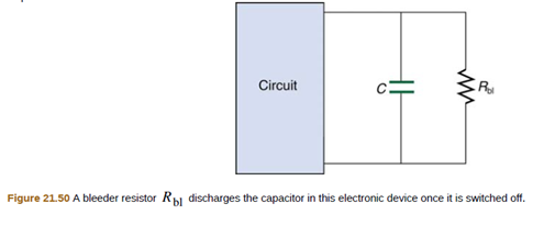
An electronic apparatus may have large capacitors at high voltage in the power supply section, presenting a shock hazard even when the apparatus is switched off. A “bleeder resistor" is therefore placed across such a capacitor, as shown schematically in Figure 21.50, to bleed the charge from it after the apparatus is off. Why must the bleeder resistance be much greater than the effective resistance of the rest of the circuit? How does this affect the time constant for discharging the capacitor?
An electronic apparatus may have large capacitors at high voltage in the power supply section, presenting a shock hazard even when the apparatus is switched off. A “bleeder resistor" is therefore placed across such a capacitor, as shown schematically in Figure 21.50, to bleed the charge from it after the apparatus is off. Why must the bleeder resistance be much greater than the effective resistance of the rest of the circuit? How does this affect the time constant for discharging the capacitor?
An electronic apparatus may have large capacitors at high voltage in the power supply section, presenting a shock hazard even when the apparatus is switched off. A “bleeder resistor" is therefore placed across such a capacitor, as shown schematically in Figure 21.50, to bleed the charge from it after the apparatus is off. Why must the bleeder resistance be much greater than the effective resistance of the rest of the circuit? How does this affect the time constant for discharging the capacitor?
How can you tell which vowel is being produced here ( “ee,” “ah,” or “oo”)? Also, how would you be able to tell for the other vowels?
You want to fabricate a soft microfluidic chip like the one below. How would you go about
fabricating this chip knowing that you are targeting a channel with a square cross-sectional
profile of 200 μm by 200 μm. What materials and steps would you use and why? Disregard the
process to form the inlet and outlet.
Square Cross Section
1. What are the key steps involved in the fabrication of a semiconductor device.
2. You are hired by a chip manufacturing company, and you are asked to prepare a silicon wafer
with the pattern below. Describe the process you would use.
High Aspect
Ratio
Trenches
Undoped Si Wafer
P-doped Si
3. You would like to deposit material within a high aspect ratio trench. What approach would you
use and why?
4. A person is setting up a small clean room space to carry out an outreach activity to educate high
school students about patterning using photolithography. They obtained a positive photoresist, a
used spin coater, a high energy light lamp for exposure and ordered a plastic transparency mask
with a pattern on it to reduce cost. Upon trying this set up multiple times they find that the full
resist gets developed, and they are unable to transfer the pattern onto the resist. Help them
troubleshoot and find out why pattern of transfer has not been successful.
5. You are given a composite…
Genetic Analysis: An Integrated Approach (3rd Edition)
Knowledge Booster
Learn more about
Need a deep-dive on the concept behind this application? Look no further. Learn more about this topic, physics and related others by exploring similar questions and additional content below.
DC Series circuits explained - The basics working principle; Author: The Engineering Mindset;https://www.youtube.com/watch?v=VV6tZ3Aqfuc;License: Standard YouTube License, CC-BY


 Principles of Physics: A Calculus-Based TextPhysicsISBN:9781133104261Author:Raymond A. Serway, John W. JewettPublisher:Cengage Learning
 College PhysicsPhysicsISBN:9781938168000Author:Paul Peter Urone, Roger HinrichsPublisher:OpenStax College
 Physics for Scientists and Engineers: Foundations...PhysicsISBN:9781133939146Author:Katz, Debora M.Publisher:Cengage Learning
 Physics for Scientists and Engineers, Technology ...PhysicsISBN:9781305116399Author:Raymond A. Serway, John W. JewettPublisher:Cengage Learning
 Glencoe Physics: Principles and Problems, Student...PhysicsISBN:9780078807213Author:Paul W. ZitzewitzPublisher:Glencoe/McGraw-Hill