
Concept explainers
Videos
a.
Explain whether the interconnection of ideal sources in the circuit in Figure P2.1 in the textbook is valid or not.
a.
Answer to Problem 1P
The interconnection of ideal sources in the given circuit is valid.
Explanation of Solution
Given data:
Refer to Figure P2.1 in the textbook for required data.
Description:
All the sources in the given circuit are independent sources. The independent voltage source can carry any current that required by the connection and the independent current source can support any voltage that required by the connection.
As the given circuit consists of all ideal independent sources and the Kirchhoff’s law is not violated, the interconnection of ideal sources in the given circuit is valid.
Conclusion:
Thus, the interconnection of ideal sources in the given circuit is valid.
b.
Identify the power developing sources and power absorbed sources in the given circuit.
b.
Answer to Problem 1P
The power developing sources are 15 V voltage source and 5 A current source, and the power absorbing source is 20 V voltage source.
Explanation of Solution
Formula used:
Write the expression for power developed or absorbed by the source (voltage or current) as follows:
Here,
Calculation:
If the current enters from the negative terminal and leaves from the positive terminal of a voltage source then the source delivers the power. The delivering power is obtained with negative sign.
If the current enters from the positive terminal and leaves from the negative terminal of a voltage source then the source absorbs the power. The absorbing power is obtained with positive sign.
From the given circuit, current of 5 A enters from the positive terminal of 20 V source. Therefore, 20 V voltage source absorbs the power.
Rewrite the expression in Equation (1) to find the power absorbed by the 20 V voltage source as follows:
From given circuit, the values of
Therefore, the power absorbed by the 20 V voltage source is 100 W.
From the given circuit, current of 5 A enters from the negative terminal of 15 V source. Therefore, 15 V voltage source develops the power.
Rewrite the expression in Equation (1) to find the power developed by the 15 V voltage source as follows:
From given circuit, the values of
Therefore, the power developed by the 15 V voltage source is
From the given circuit, the voltage drop across 5 A current source is calculated by using KVL to the circuit as follows:
Therefore, the voltage drop across 5 A current source is
Rewrite the expression in Equation (1) to find the power developed by the 5 A current source as follows:
From given circuit, the values of
The negative sign indicates the developed power by the source. Therefore, the power developed by the 5 A current source is 25 W.
Conclusion:
Thus, the power developing sources are 15 V voltage source and 5 A current source, and the power absorbing source is 20 V voltage source.
c.
Verify the power absorbed in the circuit is equal to the power developed in the circuit.
c.
Answer to Problem 1P
The power absorbed in the circuit is equal to the power developed in the circuit.
Explanation of Solution
Calculation:
From Part (b), write the expression for power absorbed in the circuit as follows:
Substitute 100 W for
From Part (b), the power developed in the circuit as follows:
Substitute 75 W for
From the calculation, it is clear that the power absorbed in the circuit is equal to the power developed in the circuit.
Conclusion:
Thus, the power absorbed in the circuit is equal to the power developed in the circuit.
d.
Explain whether the interconnection of ideal sources in the modified circuit is valid or not and identify the power developing and absorbing sources in the modified circuit. Verify the power absorbed in the modified circuit is equal to the power delivered in the circuit.
d.
Answer to Problem 1P
The interconnection of ideal sources in the modified circuit is valid, voltage source of 20 V and voltage source of 15 V are power developing sources and 5 A current source is a power absorbing source. The power absorbed in the modified circuit is equal to the power developed in the circuit.
Explanation of Solution
Description:
Redraw the circuit by reversing the polarity of 20 V voltage source as shown in Figure 1.
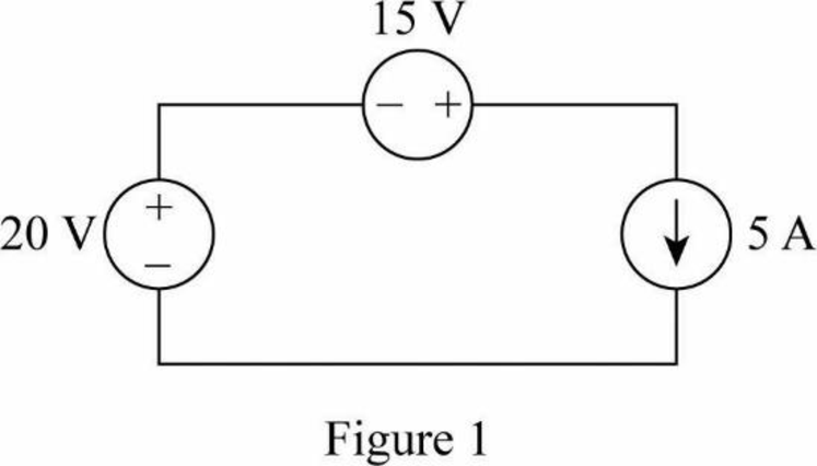
As the modified circuit in Figure 1 consists of all ideal independent sources, the interconnection of ideal sources in the modified circuit is valid.
From Figure 1, current of 5 A enters from the negative terminal of 20 V source. Therefore, 20 V voltage source develops the power.
Rewrite the expression in Equation (1) to find the power developed by the 20 V voltage source as follows:
From given circuit, the values of
Therefore, the power delivered by the 20 V voltage source is 100 W.
From the given circuit, current of 5 A enters from the negative terminal of 15 V source. Therefore, 15 V voltage source develops the power.
Rewrite the expression in Equation (1) to find the power developed by the 15 V voltage source as follows:
From given circuit, the values of
Therefore, the power developed by the 15 V voltage source is 75 W.
From the given circuit, the voltage drop across 5 A current source is calculated by using KVL to the circuit as follows:
Therefore, the voltage drop across 5 A current source is 35 V. That is, current 5 A enters the positive terminal and leaves from the negative terminal of 35 V voltage drop. Therefore, 5 A current source absorbs the power.
Rewrite the expression in Equation (1) to find the power absorbed by the 5 A current source as follows:
From given circuit, the values of
Therefore, the power absorbed by the 5 A current source is 175 W.
From the calculation, write the expression for power absorbed in the circuit as follows:
Substitute 175 W for
From the calculation, the power developed in the circuit as follows.
Substitute 100 W for
From the calculation, it is clear that the power absorbed in the circuit is equal to the power developed in the circuit.
Conclusion:
Thus, the interconnection of ideal sources in the modified circuit is valid, voltage source of 20 V and voltage source of 15 V are power developing sources and 5 A current source is a power absorbing source. The power absorbed in the modified circuit is equal to the power developed in the circuit.
Want to see more full solutions like this?
Chapter 2 Solutions
Electrical Circuits and Modified MasteringEngineering - With Access


- The efficiency of a motor is always low when it operates at 10 percent of its nominal power rating. Explain.arrow_forwardA dc motor connected to a 240 V line pro- duces a mechanical output of 160 hp. Knowing that the losses are 12 kW, calculate the input power and the line current.arrow_forwardA 115 V dc generator delivers 120 A to a load. If the generator has an efficiency of 81 percent, calculate the mechanical power needed to drive it [hp].arrow_forward
- A machine having class B insulation attains a temperature of 208°C (by resistance) in a torrid ambient temperature of 180°C. a. What is the temperature rise? b. Is the machine running too hot and, if so, by how much?arrow_forward1 Name the losses in a dc motor. 2 What causes iron losses and how can they be reduced? -3 Explain why the temperature of a machine increases as the load increases.arrow_forward20. A tractor weighing 14 kN with a wheel base of 3m carries an 8 kN load on its rear wheel. Compute the maximum bending moment and shear when crossing a 4.5 span. Consider the load only at the wheels.arrow_forward
- A 110-V, three-phase, Y-connected, 8 pole, 48-slot, 6000-rpm, double-layer wound chronoun anı vonorotor boo 10 +1 urn or oilarrow_forward-7 Name some of the factors that contribute to the deterioration of organic insulators. -8 A motor is built with class H insulation. What maximum hot-spot temperature can it withstand?arrow_forwardCalculate the full-load current of a 250 hp, 230 V dc motor having an efficiency of 92 percent.arrow_forward
- Assignment #2 A 110-V, three-phase, Y-connected, 8 pole, 48-slot, 6000-rpm, double-layer wound, synchronous generator has 12 turns per coil. If one side of the coil is in slot 1, the other side is in slot 6. There are 4 parallel paths. When the generator delivers the rated load at a line voltage of 110 V, the voltage regulation is 5%. What is the flux per pole? Draw two consecutive phasegroups of one of the phase windings and connect them (a) in series and (b) in parallel showing the Start (S) and Finish (F) of both connections. (A separate drawing for each connection)arrow_forward3-4 Transmissiva Live of 120km has R= 0.2 ~2/15 X= 0.8 -2/km Y = 15H/6 5/km The line is supplies a load of 45 kV, SOMW, 0.8 lead p.f find sending voltage, Sending Current p.f. Sanding Voltage Regulation ⑨Voltage 5 Ⓒ charching coming! изу usy π cct लेarrow_forwardA (medium) single phase transmission line 100 km long has the following constants : Resistance/km = 0.25 Q; Susceptance/km = 14 × 10° siemen ; Reactance/km = 0.8 Receiving end line voltage = 66,000 V Assuming that the total capacitance of the line is localised at the receiving end alone, determine (i) the sending end current (ii) the sending end voltage (iii) regulation and (iv) supply power factor. The line is delivering 15,000 kW at 0.8 power factor Lead Draw the phasor diagram to illustrate your calculations.arrow_forward
 Introductory Circuit Analysis (13th Edition)Electrical EngineeringISBN:9780133923605Author:Robert L. BoylestadPublisher:PEARSON
 Delmar's Standard Textbook Of ElectricityElectrical EngineeringISBN:9781337900348Author:Stephen L. HermanPublisher:Cengage Learning
 Programmable Logic ControllersElectrical EngineeringISBN:9780073373843Author:Frank D. PetruzellaPublisher:McGraw-Hill Education
 Fundamentals of Electric CircuitsElectrical EngineeringISBN:9780078028229Author:Charles K Alexander, Matthew SadikuPublisher:McGraw-Hill Education
 Electric Circuits. (11th Edition)Electrical EngineeringISBN:9780134746968Author:James W. Nilsson, Susan RiedelPublisher:PEARSON
 Engineering ElectromagneticsElectrical EngineeringISBN:9780078028151Author:Hayt, William H. (william Hart), Jr, BUCK, John A.Publisher:Mcgraw-hill Education,