
Concept explainers
Videos
a.
Explain whether the interconnection of ideal sources in the circuit in Figure P2.1 in the textbook is valid or not.
a.
Answer to Problem 1P
The interconnection of ideal sources in the given circuit is valid.
Explanation of Solution
Given data:
Refer to Figure P2.1 in the textbook for required data.
Description:
All the sources in the given circuit are independent sources. The independent voltage source can carry any current that required by the connection and the independent current source can support any voltage that required by the connection.
As the given circuit consists of all ideal independent sources and the Kirchhoff’s law is not violated, the interconnection of ideal sources in the given circuit is valid.
Conclusion:
Thus, the interconnection of ideal sources in the given circuit is valid.
b.
Identify the power developing sources and power absorbed sources in the given circuit.
b.
Answer to Problem 1P
The power developing sources are 15 V voltage source and 5 A current source, and the power absorbing source is 20 V voltage source.
Explanation of Solution
Formula used:
Write the expression for power developed or absorbed by the source (voltage or current) as follows:
Here,
Calculation:
If the current enters from the negative terminal and leaves from the positive terminal of a voltage source then the source delivers the power. The delivering power is obtained with negative sign.
If the current enters from the positive terminal and leaves from the negative terminal of a voltage source then the source absorbs the power. The absorbing power is obtained with positive sign.
From the given circuit, current of 5 A enters from the positive terminal of 20 V source. Therefore, 20 V voltage source absorbs the power.
Rewrite the expression in Equation (1) to find the power absorbed by the 20 V voltage source as follows:
From given circuit, the values of
Therefore, the power absorbed by the 20 V voltage source is 100 W.
From the given circuit, current of 5 A enters from the negative terminal of 15 V source. Therefore, 15 V voltage source develops the power.
Rewrite the expression in Equation (1) to find the power developed by the 15 V voltage source as follows:
From given circuit, the values of
Therefore, the power developed by the 15 V voltage source is
From the given circuit, the voltage drop across 5 A current source is calculated by using KVL to the circuit as follows:
Therefore, the voltage drop across 5 A current source is
Rewrite the expression in Equation (1) to find the power developed by the 5 A current source as follows:
From given circuit, the values of
The negative sign indicates the developed power by the source. Therefore, the power developed by the 5 A current source is 25 W.
Conclusion:
Thus, the power developing sources are 15 V voltage source and 5 A current source, and the power absorbing source is 20 V voltage source.
c.
Verify the power absorbed in the circuit is equal to the power developed in the circuit.
c.
Answer to Problem 1P
The power absorbed in the circuit is equal to the power developed in the circuit.
Explanation of Solution
Calculation:
From Part (b), write the expression for power absorbed in the circuit as follows:
Substitute 100 W for
From Part (b), the power developed in the circuit as follows:
Substitute 75 W for
From the calculation, it is clear that the power absorbed in the circuit is equal to the power developed in the circuit.
Conclusion:
Thus, the power absorbed in the circuit is equal to the power developed in the circuit.
d.
Explain whether the interconnection of ideal sources in the modified circuit is valid or not and identify the power developing and absorbing sources in the modified circuit. Verify the power absorbed in the modified circuit is equal to the power delivered in the circuit.
d.
Answer to Problem 1P
The interconnection of ideal sources in the modified circuit is valid, voltage source of 20 V and voltage source of 15 V are power developing sources and 5 A current source is a power absorbing source. The power absorbed in the modified circuit is equal to the power developed in the circuit.
Explanation of Solution
Description:
Redraw the circuit by reversing the polarity of 20 V voltage source as shown in Figure 1.
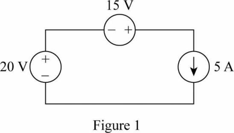
As the modified circuit in Figure 1 consists of all ideal independent sources, the interconnection of ideal sources in the modified circuit is valid.
From Figure 1, current of 5 A enters from the negative terminal of 20 V source. Therefore, 20 V voltage source develops the power.
Rewrite the expression in Equation (1) to find the power developed by the 20 V voltage source as follows:
From given circuit, the values of
Therefore, the power delivered by the 20 V voltage source is 100 W.
From the given circuit, current of 5 A enters from the negative terminal of 15 V source. Therefore, 15 V voltage source develops the power.
Rewrite the expression in Equation (1) to find the power developed by the 15 V voltage source as follows:
From given circuit, the values of
Therefore, the power developed by the 15 V voltage source is 75 W.
From the given circuit, the voltage drop across 5 A current source is calculated by using KVL to the circuit as follows:
Therefore, the voltage drop across 5 A current source is 35 V. That is, current 5 A enters the positive terminal and leaves from the negative terminal of 35 V voltage drop. Therefore, 5 A current source absorbs the power.
Rewrite the expression in Equation (1) to find the power absorbed by the 5 A current source as follows:
From given circuit, the values of
Therefore, the power absorbed by the 5 A current source is 175 W.
From the calculation, write the expression for power absorbed in the circuit as follows:
Substitute 175 W for
From the calculation, the power developed in the circuit as follows.
Substitute 100 W for
From the calculation, it is clear that the power absorbed in the circuit is equal to the power developed in the circuit.
Conclusion:
Thus, the interconnection of ideal sources in the modified circuit is valid, voltage source of 20 V and voltage source of 15 V are power developing sources and 5 A current source is a power absorbing source. The power absorbed in the modified circuit is equal to the power developed in the circuit.
Want to see more full solutions like this?
Chapter 2 Solutions
Electric Circuits (10th Edition)


- can you show me full workings for this problem. the solution is - v0 = 10i2 = 2.941 volts, i0 = i1 – i2 = (5/3)i2 = 490.2mA.arrow_forwardQ4. a) Consider a transmission line modelled as a four-terminal network with an unknown configuration. You are provided with the following measured parameters at the operating frequency: Open-circuit voltage ratio: 0.9521° • Short-circuit impedance: 40+j80 • Open-circuit admittance: -j2 × 10-4 S Use the four terminal equations and the provided measurements to mathematically derive the A, B, C, and D parameters of the network and explain their physical significance. Show your work and formulas used in the derivation.arrow_forwardQ1. Consider a single-phase step-down transformer with primary and secondary turns of 600 and 100 respectively and a primary voltage of 11 kV. (i) An open circuit test was conducted on the transformer and the primary current was measured as: I₁ = 2.20 A Use these results to calculate the magnetising reactance in the equivalent circuit (X) given that Rm, representing the core loss, has a value of 21 km. (ii) The remaining equivalent circuit parameters are as follows: R₁ = 40, X₁ = 25 N, R₂ = 0.4 N, X₂ = 0.3 N Draw the complete simplified equivalent circuit, by referring series components on the primary side to the secondary, giving all component values. (iii) The transformer is connected, on its secondary side, to a load of 10 at a power factor of 1. Calculate the voltage across the load. (iv) Calculate the efficiency of the transformer when operating at the load given in part (iii).arrow_forward
- b) A 132 kV supply feeds a line of reactance 15 which is connected to a 100 MVA, 132/33 kV transformer of 0.08 p.u. reactance as shown in the Figure 2. The transformer feeds a 33 kV line of reactance 8 Q, which, in turn, is connected to a 75 MVA, 33/11 KV transformer of 0.12 p.u. reactance. The transformer supplies an 11 KV substation from which a local 11 kV feeder of 4 Q reactance is supplied. T1 T2 132 kV 33 kV 11 kV Fault X CB Relay Figure 2. Network for Q4 b). (i) Given the system base of 100 MVA, compute the total equivalent reactance of the radial circuit in per unit (p.u.). (ii) Determine the three-phase fault current at the load end of the 11 kV feeder, assuming a fault impedance of 0.05 Q. Calculate the fault current in Amperes. (iii) The 11 kV feeder connects to a protective overcurrent relay via 200/5 A current transformers. This relay has a standard normally inverse IDMT characteristic, with a setting current of 3 A and a time multiplier setting of 0.4. Calculate the…arrow_forwardQ2. a) Two three-phase transformers, designated A and B, have the following secondary equivalent circuit parameters per phase: R₁ = 0.002 Q, XA = 0.03 Q, RB = 0.004 Q, X = 0.012 Q Transformer A is 250 kVA and transformer B is 450 kVA. Calculate how they share a load of 650 KVA when connected in parallel (assume the voltage ratios are equal) b) A step-up transformer is being specified for the beginning of a 3-phase, 4 wire high voltage transmission line. Discuss your recommendation for the configuration of the transformer connections on both the primary and secondary side of the transformer. c) Define power system protection and describe its fundamental purpose. Discuss the following key concepts including discrimination, stability, speed of operation, sensitivity, and reliability in the context of the power system protection components and schemes.arrow_forwardQ3. a) Given the unsymmetrical phasors for a three-phase system, they can be represented in terms of their symmetrical components as follows: [Fa] [1 1 Fb = 1 a² [Fc. 11[Fao] a Fai 1 a a2F a2- where F stands for any three-phase quantity. Conversely, the sequence components can be derived from the unsymmetrical phasors as: [11 1] [Fal Faol Fa1 = 1 a a² F 1 a² a a2. Given the unbalanced three-phase voltages: V₁ = 120/10° V, V₂ = 200/110° V, V = 240/200° V Calculate in polar form the sequence components of the voltage.arrow_forward
- Complete the table of values for this circuit:arrow_forward*P2.58. Solve for the node voltages shown in Figure P2.58. - 10 Ω w + 10 Ω 15 Ω w w '+' 5 Ω 20x 1 A Figure P2.58 w V2 502 12Aarrow_forwardAn 18.65 kW, 4-pole, 50 Hz, 3-phase induction motor has friction and windage losses of 2.5% of the output. The full-load slip is 4%. Find for full-load (i) the rotor cu loss (ii) the rotor input power (iii) the output torque.arrow_forward
- Q1: Consider the finite state machine logic implementation in Fig. shown below: a. b. Construct the state diagram. Repeat the circuit design using j-k flip flop. C'lk A D 10 Clk Q D 32 Cik O 31 Please solve the question on a sheet of paper by hand and explain everything related to the question step by step.arrow_forwardAnot ined sove in peaper S PU +96 An 18.65 kW, 4-pole, 50 Hz, 3-phase induction motor has friction and windage losses of 2.5% of the output. The full-load slip is 4 %. Find for full-load (i) the rotor cu loss (ii) the rotor input power (iii) the output torque. 750 1 T el Marrow_forwardAlternator has star-connected,4-pole, 50 Hz as the following data: Flux per pole-0.12 Wb; No. of slot/pole/phase=4; conductor/slot=4; Each coil spans 150° (electrical degree) pitches Find (i) number of turns per phase (ii) distribution factor (iii) pitch factor (iv) no-load phase voltage (v) no-load line voltage.arrow_forward
 Introductory Circuit Analysis (13th Edition)Electrical EngineeringISBN:9780133923605Author:Robert L. BoylestadPublisher:PEARSON
 Delmar's Standard Textbook Of ElectricityElectrical EngineeringISBN:9781337900348Author:Stephen L. HermanPublisher:Cengage Learning
 Programmable Logic ControllersElectrical EngineeringISBN:9780073373843Author:Frank D. PetruzellaPublisher:McGraw-Hill Education
 Fundamentals of Electric CircuitsElectrical EngineeringISBN:9780078028229Author:Charles K Alexander, Matthew SadikuPublisher:McGraw-Hill Education
 Electric Circuits. (11th Edition)Electrical EngineeringISBN:9780134746968Author:James W. Nilsson, Susan RiedelPublisher:PEARSON
 Engineering ElectromagneticsElectrical EngineeringISBN:9780078028151Author:Hayt, William H. (william Hart), Jr, BUCK, John A.Publisher:Mcgraw-hill Education,