
Concept explainers
Videos
The value of the CT secondary current (I’) and VT secondary voltage (V’).
Answer to Problem 10.1P
Explanation of Solution
Given Information:
Calculation:
The secondary voltage of the voltage transformer (V’) is,
Substitute the values in the above equation,
Now, the current (I) entering the primary of the current transformer is,
On substituting the values in the above equation,
And get,
Here, the CT equivalent circuit is,
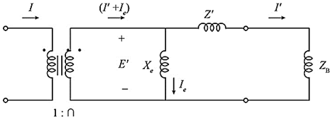
Fig: CT equivalent circuit diagram
Now, the secondary current of CT is,
Substituting the values in the above equation,
From the above equivalent circuit diagram, the secondary current consists of two components, there are
Whereas, I’ is the relay current and Ie is the exciting current.
CT error is Zero in the given question.
So that the exciting current is Zero, (Ie=0), therefore,
Want to see more full solutions like this?
Chapter 10 Solutions
EBK POWER SYSTEM ANALYSIS AND DESIGN


- solve this, show all steps, no ai pz, please draw it outarrow_forwardNO AI PLEASE WILL REJECTarrow_forward"?Can the expert help me solve only a bonus question using Arduino" The system must control 3 LEDs (Red, Green, and Blue) to operate in 4 different lighting modes: Mode 3: LEDs fade in and out smoothly (PWM control) in the order Red Green → Blue. Bonus Challenge (Potentiometer Control): The potentiometer (connected to pin A0) allows for dynamic control of the brightness during the fading mode (Mode 3). This allows the user to adjust how bright or dim the LEDs should fade in and out. This solution meets the project requirements, including the current limits, and provides interactive functionality with the push button and potentiometer.arrow_forward
- See the attached image for answeringarrow_forwardI need a complete and correct solution, please Suppose that X and Y have the following joint probability distribution y 24 1 [0.1 0.15] P(X,Y) = x3 0.2 0.3 50.1 0.15] a) Evaluate the marginal distribution of X and Y b) Find P(Y/X) and P(X/Y). c) Find P(Y=2/X=3). d) Find μx, Hy, σ,σ and oxy.arrow_forwardSuppose that X and Y have the following joint probability distribution 2 1 [0.1 y 4 0.151 P(X,Y) = x3 0.2 0.3 50.1 0.15 a) Evaluate the marginal distribution of X and Y. b) Find P(Y/X) and P(X/Y). c) Find P(Y=2/X=3). d) Find μx, μy, σ,σ and oxy.arrow_forward
- Prelab Information Laboratory Preliminary Discussion Second-order RLC Circuit Analysis The second-order RLC circuit shown in figure 1 below represents all voltages and impedances as functions of the complex variable, s. Note, of course, that the impedances associated with R, RL, and Rs are constant independent of frequency, so the 's' notation is omitted. Again, one of the advantages of s-domain analysis is that we can apply all of the circuit analysis techniques learned for AC and DC circuits. ZI(s) Zc(s) Rs w RL ww + + VRS(S) VRL(S) VL(s) Vc(s) VR(S) R Vs(s) Figure 1: A second-order RLC circuit represented in the s-domain. To generate the s-domain expression for the output voltage, Vout(s) = VR(S), for the circuit shown in figure 1, we can apply voltage division in the s-domain as shown in equation 1 below. For equation 1 we define the following circuit parameters. RT=RS + RL + R where: R₁ = Total series resistance Rs Signal generator output resistance (fixed) Inductor internal…arrow_forwardCan you show how the correct answer was found.arrow_forwardFor the circuit shown in Figure (1). Solve the following: ( A. What type of logic does it represent? C. Explain the function of D1. B. What type of logic family does it belong to? D. Explain the importance of DL. E. How many stages it has? Explain the function of each one. F. Construct the truth table and explain it briefly. G.How can you convert this circuit to an open collector form? Explain and sketch it. H.How can you convert this circuit to a tri-state form? Explain and sketch it. I. How can you prevent the transistors from being saturated? J. Which transistor should be modified to convert this circuit to a 4-inputs NAND? Explain and sketch it. K.Convert this circuit to a 2-inputs NOR gate and draw it. R-1200 R-4.2K R-1.5K R-IK Figure (1) lour e Yourarrow_forward
- E. How many stages it has? Explain the function of each one. F. Construct the truth table and explain it briefly. G.How can you convert this circuit to an open collector form? Explain and sketch it. H.How can you convert this circuit to a tri-state form? Explain and sketch it. I. How can you prevent the transistors from being saturated? J. Which transistor should be modified to convert this circuit to a 4-inputs NAND? Explain and sketch it. K.Convert this circuit to a 2-inputs NOR gate and draw it. R-4.2K W R-1200 R-1.5K R-IK Figure (1) JOUT e Yourarrow_forward1. Determine the z-transform, including the region of convergence (ROC), of the following signals: a)x[n={3,0,0,0,0,51-4} b) x2[n] = ((1/3)^n ,n ≥0 2", n < 0 c) X3[n]= (1/3)^n- 2", n ≥ 0 0, n < 0arrow_forwardUse ECL configuration to realize a 2-inputs OR /NOR gate and verify its function using the truth table, showing the state of each transistor in the circuit. Assume Vcc 5V, VEE-0V & VREF=1.5V.arrow_forward
 Power System Analysis and Design (MindTap Course ...Electrical EngineeringISBN:9781305632134Author:J. Duncan Glover, Thomas Overbye, Mulukutla S. SarmaPublisher:Cengage Learning