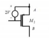
What is the minimum value of V for which this MOS is saturated? Clearly identify types of transistors, drain and source terminals, calculate with and w/o body bias
What is the minimum value of V for which this MOS is saturated? Clearly identify types of transistors, drain and source terminals, calculate with and w/o body bias
Introductory Circuit Analysis (13th Edition)
13th Edition
ISBN:9780133923605
Author:Robert L. Boylestad
Publisher:Robert L. Boylestad
Chapter1: Introduction
Section: Chapter Questions
Problem 1P: Visit your local library (at school or home) and describe the extent to which it provides literature...
Related questions
Question

Transcribed Image Text:The image contains a question related to MOS (Metal-Oxide-Semiconductor) transistors.
**Question:**
What is the minimum value of \( V_{AB} \) for which this MOS is saturated?
**Circuit Diagram:**
- There is a voltage source of \( 2V \) connected to the gate of the MOS transistor.
- The MOS transistor is labeled as \( M_3 \).
- The source terminal is connected to a point labeled \( B \) and the drain terminal is connected to a point labeled \( A \).
Additional instructions are provided to:
- Clearly identify the types of transistors, drain, and source terminals.
- Calculate with and without body bias.

Transcribed Image Text:### MOSFET Parameters Table
This table outlines the parameters for NMOS and PMOS transistors, crucial for understanding MOSFET operation in various applications.
| MOSFET Parameter | NMOS | PMOS | Units |
|------------------|------|------|-----------|
| K or K' | 24 | 8 | μA/V² |
| Vₜ₀ | 0.75 | -0.75| V |
| γ | 0.8 | 0.4 | V¹/² |
| φ | 0.6 | 0.6 | V |
| λ | 0.01 | 0.02 | V⁻¹ |
#### Explanation:
- **K or K' (Transconductance parameter):** Measures the amplification ability of the MOSFET. Higher values in NMOS (24 μA/V²) compared to PMOS (8 μA/V²) suggest stronger current-driving capacity.
- **Vₜ₀ (Threshold Voltage):** The minimum gate-to-source voltage required to create a conducting path between the source and drain. Positive for NMOS (0.75 V), negative for PMOS (-0.75 V).
- **γ (Body effect coefficient):** Reflects the change in threshold voltage due to a change in the substrate (body) bias. The NMOS has a higher γ (0.8 V¹/²) compared to PMOS (0.4 V¹/²).
- **φ (Surface potential):** Indicates the required surface potential to invert the semiconductor surface. It is equal for both NMOS and PMOS at 0.6 V.
- **λ (Channel length modulation parameter):** Describes the variation of the drain current with the drain-to-source voltage beyond saturation. Slightly higher in PMOS (0.02 V⁻¹) than NMOS (0.01 V⁻¹).
Expert Solution
Step 1
The MOS is as shown below,

We need to find the minimum value of VAB for which the MOSFET is saturated, with and without body bias effect.
Step by step
Solved in 3 steps with 2 images

Recommended textbooks for you

Introductory Circuit Analysis (13th Edition)
Electrical Engineering
ISBN:
9780133923605
Author:
Robert L. Boylestad
Publisher:
PEARSON

Delmar's Standard Textbook Of Electricity
Electrical Engineering
ISBN:
9781337900348
Author:
Stephen L. Herman
Publisher:
Cengage Learning

Programmable Logic Controllers
Electrical Engineering
ISBN:
9780073373843
Author:
Frank D. Petruzella
Publisher:
McGraw-Hill Education

Introductory Circuit Analysis (13th Edition)
Electrical Engineering
ISBN:
9780133923605
Author:
Robert L. Boylestad
Publisher:
PEARSON

Delmar's Standard Textbook Of Electricity
Electrical Engineering
ISBN:
9781337900348
Author:
Stephen L. Herman
Publisher:
Cengage Learning

Programmable Logic Controllers
Electrical Engineering
ISBN:
9780073373843
Author:
Frank D. Petruzella
Publisher:
McGraw-Hill Education

Fundamentals of Electric Circuits
Electrical Engineering
ISBN:
9780078028229
Author:
Charles K Alexander, Matthew Sadiku
Publisher:
McGraw-Hill Education

Electric Circuits. (11th Edition)
Electrical Engineering
ISBN:
9780134746968
Author:
James W. Nilsson, Susan Riedel
Publisher:
PEARSON

Engineering Electromagnetics
Electrical Engineering
ISBN:
9780078028151
Author:
Hayt, William H. (william Hart), Jr, BUCK, John A.
Publisher:
Mcgraw-hill Education,