V DD M,(20/1) R R M,(10/1) V V ss Fig 6. Amplifier w/ active load

Introductory Circuit Analysis (13th Edition)
13th Edition
ISBN:9780133923605
Author:Robert L. Boylestad
Publisher:Robert L. Boylestad
Chapter1: Introduction
Section: Chapter Questions
Problem 1P: Visit your local library (at school or home) and describe the extent to which it provides literature...

Related questions
Question

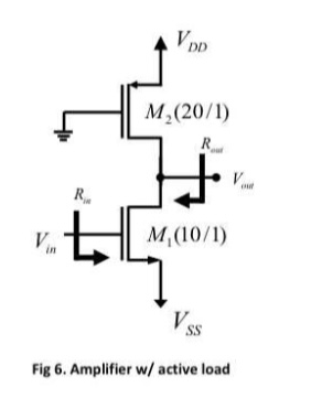
Transcribed Image Text:**Assume M1 and M2 are saturated**
(a) Find expressions for small signal parameters
(b) If the DC current flowing through both transistors is 50 µA, numerically evaluate the expressions found in (a)
**Diagram Explanation:**
The diagram shows an amplifier with an active load. The key components and connections are as follows:
- **M1 and M2 Transistors**:
- M1 has a width to length ratio of (10/1).
- M2 has a width to length ratio of (20/1).
- **Connections**:
- Both transistors are shown in a configuration typical for amplifiers where M1 operates as the amplifying transistor and M2 as the load.
- V_in is applied to the gate of M1.
- V_out is taken between the drain of M1 and the source of M2.
- The gate of M2 is connected to its drain, establishing it as a diode-connected transistor.
- **Voltage Sources**:
- V_DD is the positive supply voltage connected to the source of M2.
- V_SS is the negative supply voltage connected to the source of M1.
- **Resistors**:
- R_in is shown at the gate of M1.
- R_load is shown at the output between M1 and M2.
**Figure 6: Amplifier with active load**

Transcribed Image Text:### MOSFET Parameters for NMOS and PMOS
This table provides a comparison of key parameters for NMOS and PMOS transistors, essential components in electronic circuits. Understanding these parameters is critical for modeling and designing MOSFET-based circuits.
| MOSFET Parameter | NMOS | PMOS | Units |
|------------------|------|------|-----------|
| K or K’ | 24 | 8 | µA/V² |
| Vᵀ₀ | 0.75 | -0.75| V |
| γ (Gamma) | 0.8 | 0.4 | V¹/² |
| φ (Phi) | 0.6 | 0.6 | V |
| λ (Lambda) | 0.01 | 0.02 | V⁻¹ |
#### Explanation of Parameters:
- **K or K’ (Transconductance Parameter):** This measures the transistor's ability to conduct. Higher values indicate better conduction efficiency. NMOS transistors have a K value of 24 µA/V², while PMOS transistors have a lower value of 8 µA/V².
- **Vᵀ₀ (Threshold Voltage):** This is the minimum gate-to-source voltage required to create a conducting path between the source and drain terminals. NMOS has a Vᵀ₀ of 0.75 V, and PMOS has a Vᵀ₀ of -0.75 V, reflecting the polarity difference.
- **γ (Gamma, Body Effect Coefficient):** This parameter indicates how the threshold voltage changes with the substrate bias. It is 0.8 V¹/² for NMOS and 0.4 V¹/² for PMOS.
- **φ (Phi, Surface Potential):** Represents the voltage potential at the silicon surface and is the same for both NMOS and PMOS at 0.6 V.
- **λ (Lambda, Channel-Length Modulation Parameter):** Describes the change in drain current with drain-source voltage due to the shortening of the effective channel length. NMOS transistors have a λ value of 0.01 V⁻¹, whereas PMOS transistors have a value of 0.02 V⁻¹.
Understanding these parameters helps in designing precise and efficient electronic circuits using NMOS
Expert Solution
Step 1
The given circuit diagram is shown below:

Step by step
Solved in 4 steps with 2 images

Similar questions
Recommended textbooks for you
Introductory Circuit Analysis (13th Edition)
Electrical Engineering
ISBN:
9780133923605
Author:
Robert L. Boylestad
Publisher:
PEARSON

Delmar's Standard Textbook Of Electricity
Electrical Engineering
ISBN:
9781337900348
Author:
Stephen L. Herman
Publisher:
Cengage Learning

Programmable Logic Controllers
Electrical Engineering
ISBN:
9780073373843
Author:
Frank D. Petruzella
Publisher:
McGraw-Hill Education
Introductory Circuit Analysis (13th Edition)
Electrical Engineering
ISBN:
9780133923605
Author:
Robert L. Boylestad
Publisher:
PEARSON
Delmar's Standard Textbook Of Electricity
Electrical Engineering
ISBN:
9781337900348
Author:
Stephen L. Herman
Publisher:
Cengage Learning
Programmable Logic Controllers
Electrical Engineering
ISBN:
9780073373843
Author:
Frank D. Petruzella
Publisher:
McGraw-Hill Education

Fundamentals of Electric Circuits
Electrical Engineering
ISBN:
9780078028229
Author:
Charles K Alexander, Matthew Sadiku
Publisher:
McGraw-Hill Education

Electric Circuits. (11th Edition)
Electrical Engineering
ISBN:
9780134746968
Author:
James W. Nilsson, Susan Riedel
Publisher:
PEARSON

Engineering Electromagnetics
Electrical Engineering
ISBN:
9780078028151
Author:
Hayt, William H. (william Hart), Jr, BUCK, John A.
Publisher:
Mcgraw-hill Education,