onsider the B My logic circuit shown below. Which of the logic expression is correct +VDD M₂ M₁ Vout= A + B Vout= AB Vout= A + B Vout= AB -O Vout
onsider the B My logic circuit shown below. Which of the logic expression is correct +VDD M₂ M₁ Vout= A + B Vout= AB Vout= A + B Vout= AB -O Vout

Introductory Circuit Analysis (13th Edition)
13th Edition
ISBN:9780133923605
Author:Robert L. Boylestad
Publisher:Robert L. Boylestad
Chapter1: Introduction
Section: Chapter Questions
Problem 1P: Visit your local library (at school or home) and describe the extent to which it provides literature...

Related questions
Question
![### CMOS Logic Circuit Analysis
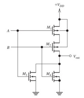
Consider the CMOS logic circuit shown below. Which of the logic expressions is correct?
#### Circuit Diagram Description
The circuit consists of four MOSFET transistors labeled \( M_1, M_2, M_3, \) and \( M_4 \). Here's a detailed explanation of the diagram:
- **Transistors \( M_1 \) and \( M_2 \)** are PMOS transistors connected in a parallel configuration, with their sources connected to a positive voltage supply \( +V_{DD} \).
- **Transistors \( M_3 \) and \( M_4 \)** are NMOS transistors connected in a series configuration, with their sources connected to the ground.
- The gates of \( M_1 \) and \( M_3 \) are both controlled by input \( A \).
- The gates of \( M_2 \) and \( M_4 \) are both controlled by input \( B \).
- The output \( V_{out} \) is taken from the connection between the PMOS network and the NMOS network.
#### Logical Expression Options
1. \( V_{out} = A + B \)
2. \( V_{out} = \overline{AB} \)
3. \( V_{out} = \overline{A + B} \)
4. \( V_{out} = AB \)
The circuit implements a logical NOR operation because:
- The PMOS transistors \( M_1 \) and \( M_2 \) are in parallel, turning on when their respective inputs are low, thereby pulling the output high.
- The NMOS transistors \( M_3 \) and \( M_4 \) are in series, turning on only when both inputs are high, thereby pulling the output low.
Therefore, the correct logic expression is:
\[ V_{out} = \overline{A + B} \]](/v2/_next/image?url=https%3A%2F%2Fcontent.bartleby.com%2Fqna-images%2Fquestion%2F06820c1f-89fb-488f-b065-5c9aac6ff99d%2Fb0eb4593-5000-4bc3-8cd6-827ca450425e%2Fikwxak_processed.png&w=3840&q=75)
Transcribed Image Text:### CMOS Logic Circuit Analysis
Consider the CMOS logic circuit shown below. Which of the logic expressions is correct?
#### Circuit Diagram Description
The circuit consists of four MOSFET transistors labeled \( M_1, M_2, M_3, \) and \( M_4 \). Here's a detailed explanation of the diagram:
- **Transistors \( M_1 \) and \( M_2 \)** are PMOS transistors connected in a parallel configuration, with their sources connected to a positive voltage supply \( +V_{DD} \).
- **Transistors \( M_3 \) and \( M_4 \)** are NMOS transistors connected in a series configuration, with their sources connected to the ground.
- The gates of \( M_1 \) and \( M_3 \) are both controlled by input \( A \).
- The gates of \( M_2 \) and \( M_4 \) are both controlled by input \( B \).
- The output \( V_{out} \) is taken from the connection between the PMOS network and the NMOS network.
#### Logical Expression Options
1. \( V_{out} = A + B \)
2. \( V_{out} = \overline{AB} \)
3. \( V_{out} = \overline{A + B} \)
4. \( V_{out} = AB \)
The circuit implements a logical NOR operation because:
- The PMOS transistors \( M_1 \) and \( M_2 \) are in parallel, turning on when their respective inputs are low, thereby pulling the output high.
- The NMOS transistors \( M_3 \) and \( M_4 \) are in series, turning on only when both inputs are high, thereby pulling the output low.
Therefore, the correct logic expression is:
\[ V_{out} = \overline{A + B} \]

Transcribed Image Text:The image presents a circuit schematic, specifically a source follower configuration, along with a multiple-choice question. The circuit includes several components:
- **Resistors:** \( R \), \( R_1 \), \( R_2 \), \( R_S \), \( R_L \)
- **Capacitors:** \( C_1 \), \( C_2 \)
- **Voltage Source:** Denoted as \( +V_{\text{DD}} \)
- **Input Signal:** Labeled \( u(t) \) leading to \( v_{\text{in}}(t) \)
- **Output Signal:** Labeled \( v_o \)
The circuit shows a common source follower configuration with biasing resistors and capacitors for coupling and bypass.
The question asks: "Consider the source follower circuit shown below. Which of the following statement is NOT true?"
Options:
- ( ) The voltage gain is slightly less than 1.
- ( ) The input impedance is large.
- ( ) The output impedance is small.
- ( ) The power gain is slightly less than 1.
Expert Solution
Step 1: Solution:
1. For given CMOS circuit identify thelogic gate.
- When A=B=0: M1=M2=ON and M3=M4=OFF. Hence,
format('truetype')%3Bfont-weight%3Anormal%3Bfont-style%3Anormal%3B%7D%3C%2Fstyle%3E%3C%2Fdefs%3E%3Ctext%20font-family%3D%22Arial%22%20font-size%3D%2216%22%20text-anchor%3D%22middle%22%20x%3D%225.5%22%20y%3D%2216%22%3EV%3C%2Ftext%3E%3Ctext%20font-family%3D%22Arial%22%20font-size%3D%2212%22%20text-anchor%3D%22middle%22%20x%3D%2219.5%22%20y%3D%2221%22%3Eout%3C%2Ftext%3E%3Ctext%20font-family%3D%22math17f39f8317fbdb1988ef4c628eb%22%20font-size%3D%2216%22%20text-anchor%3D%22middle%22%20x%3D%2236.5%22%20y%3D%2216%22%3E%3D%3C%2Ftext%3E%3Ctext%20font-family%3D%22Arial%22%20font-size%3D%2216%22%20text-anchor%3D%22middle%22%20x%3D%2250.5%22%20y%3D%2216%22%3EV%3C%2Ftext%3E%3Ctext%20font-family%3D%22Arial%22%20font-size%3D%2212%22%20text-anchor%3D%22middle%22%20x%3D%2264.5%22%20y%3D%2221%22%3EDD%3C%2Ftext%3E%3Ctext%20font-family%3D%22Arial%22%20font-size%3D%2216%22%20font-weight%3D%22bold%22%20text-anchor%3D%22middle%22%20x%3D%226.5%22%20y%3D%2245%22%3EV%3C%2Ftext%3E%3Ctext%20font-family%3D%22Arial%22%20font-size%3D%2212%22%20font-weight%3D%22bold%22%20text-anchor%3D%22middle%22%20x%3D%2221.5%22%20y%3D%2250%22%3Eout%3C%2Ftext%3E%3Ctext%20font-family%3D%22math17f39f8317fbdb1988ef4c628eb%22%20font-size%3D%2216%22%20font-weight%3D%22bold%22%20text-anchor%3D%22middle%22%20x%3D%2240.5%22%20y%3D%2245%22%3E%3D%3C%2Ftext%3E%3Ctext%20font-family%3D%22Arial%22%20font-size%3D%2216%22%20font-weight%3D%22bold%22%20text-anchor%3D%22middle%22%20x%3D%2254.5%22%20y%3D%2245%22%3E1%3C%2Ftext%3E%3C%2Fsvg%3E)

Step by step
Solved in 4 steps with 8 images

Knowledge Booster


Learn more about
Need a deep-dive on the concept behind this application? Look no further. Learn more about this topic, electrical-engineering and related others by exploring similar questions and additional content below.Recommended textbooks for you
Introductory Circuit Analysis (13th Edition)
Electrical Engineering
ISBN:
9780133923605
Author:
Robert L. Boylestad
Publisher:
PEARSON

Delmar's Standard Textbook Of Electricity
Electrical Engineering
ISBN:
9781337900348
Author:
Stephen L. Herman
Publisher:
Cengage Learning

Programmable Logic Controllers
Electrical Engineering
ISBN:
9780073373843
Author:
Frank D. Petruzella
Publisher:
McGraw-Hill Education
Introductory Circuit Analysis (13th Edition)
Electrical Engineering
ISBN:
9780133923605
Author:
Robert L. Boylestad
Publisher:
PEARSON
Delmar's Standard Textbook Of Electricity
Electrical Engineering
ISBN:
9781337900348
Author:
Stephen L. Herman
Publisher:
Cengage Learning
Programmable Logic Controllers
Electrical Engineering
ISBN:
9780073373843
Author:
Frank D. Petruzella
Publisher:
McGraw-Hill Education

Fundamentals of Electric Circuits
Electrical Engineering
ISBN:
9780078028229
Author:
Charles K Alexander, Matthew Sadiku
Publisher:
McGraw-Hill Education

Electric Circuits. (11th Edition)
Electrical Engineering
ISBN:
9780134746968
Author:
James W. Nilsson, Susan Riedel
Publisher:
PEARSON

Engineering Electromagnetics
Electrical Engineering
ISBN:
9780078028151
Author:
Hayt, William H. (william Hart), Jr, BUCK, John A.
Publisher:
Mcgraw-hill Education,