Explore layout of CMOS inverters and logic gates.
Explore layout of CMOS inverters and logic gates.
The circuit of CMOS inverter is made with one nMOS and one pMOS transistor. but the combinations of this two can be used differently to design the circuit.

CMOS Inverter Circuit

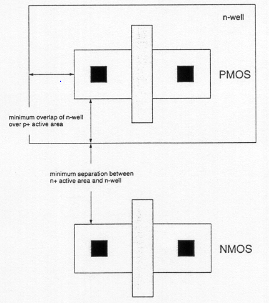
Positioning of one nMOS and one pMOS transistor.
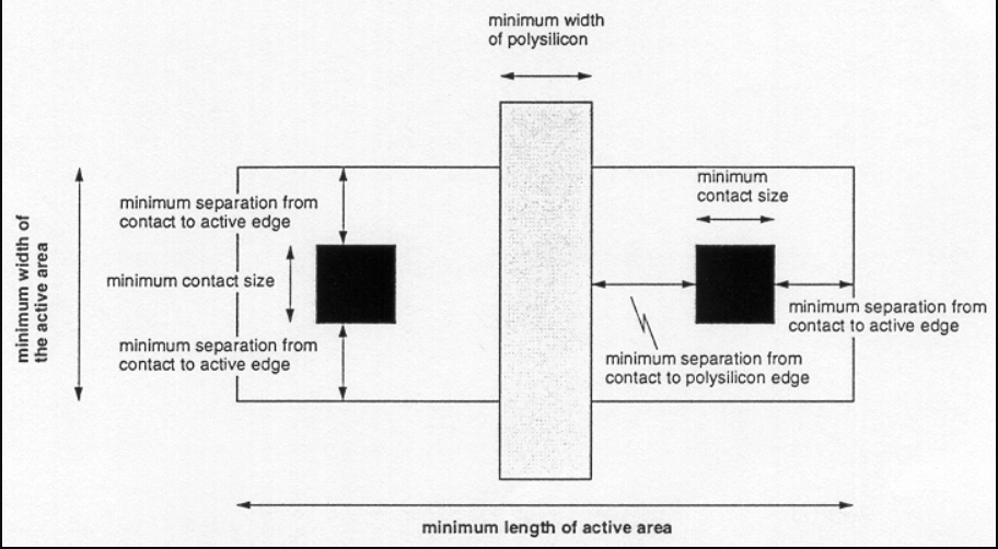
While designing the circuit layout, every single transistor is designed individually with design rules. for the design width of the polysilicon line over the active area (which is the gate of the transistor) is typically taken as the minimum poly width as shown in above figure.
The overall active area can be determine by the following formula:
The pMOS transistor must be placed in an n-well region, and the minimum size of the n- well is dictated by the pMOS active area and the minimum n-well overlap over n+.
The separation between the nMOS and the pMOS transistor is determined by the minimum distance between the n+ active area and the n-well shown in positioning diagram.
The polysilicon gates of the pMOS and the nMOS transistors are generally aligned.
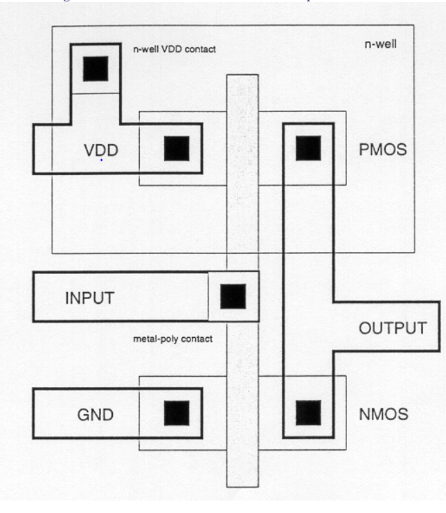
the diagram shown below shows the nections in metal, for the output node and for the VDD and GND contacts which finalize the layout.
VDD contact must be present in n-well region for the proper biasing.

Detail layout of CMOS inverter.
Step by step
Solved in 3 steps with 4 images


