Design a Single cell -1 bit Carry propagate (Ripple Carry Adder) full adder. A. Generate the truth tableb. B. Using K-map, determine the logical expression for Carry out (C-out) and Sum (S) C.Based on the logical expression, create the schematic diagram for full adder


Design a Single cell -1 bit Carry propagate (Ripple Carry Adder) full adder.
A. Generate the truth tableb.
B. Using K-map, determine the logical expression for Carry out (C-out) and Sum (S)
C.Based on the logical expression, create the schematic diagram for full adder
Ripple carry adder circuit:
Multiple full adder circuits can be cascaded in parallel to add an N-bit number. For an N- bit parallel adder, there must be N number of full adder circuits. A ripple carry adder is a logic circuit in which the carry-out of each full adder is the carry in of the succeeding next most significant full adder. It is called a ripple carry adder because each carry bit gets rippled into the next stage. In a ripple carry adder the sum and carry out bits of any half adder stage is not valid until the carry in of that stage occurs.Propagation delays inside the logic circuitry is the reason behind this. Propagation delay is time elapsed between the application of an input and occurance of the corresponding output. Consider a NOT gate, When the input is “0” the output will be “1” and vice versa. The time taken for the NOT gate’s output to become “0” after the application of logic “1” to the NOT gate’s input is the propagation delay here. Similarly the carry propagation delay is the time elapsed between the application of the carry in signal and the occurance of the carry out (Cout) signal. Circuit diagram of a 4-bit ripple carry adder is shown below.
Ripple full adder
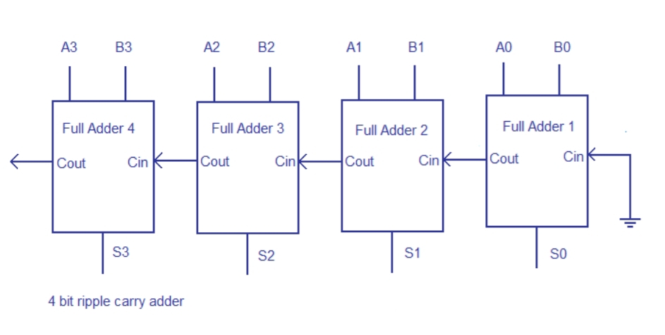 Sum out S0 and carry out Cout of the Full Adder 1 is valid only after the propagation delay of Full Adder 1. In the same way, Sum out S3 of the Full Adder 4 is valid only after the joint propagation delays of Full Adder 1 to Full Adder 4. In simple words, the final result of the ripple carry adder is valid only after the joint propogation delays of all full adder circuits inside it.

Trending now
This is a popular solution!

Step by step
Solved in 3 steps with 3 images


