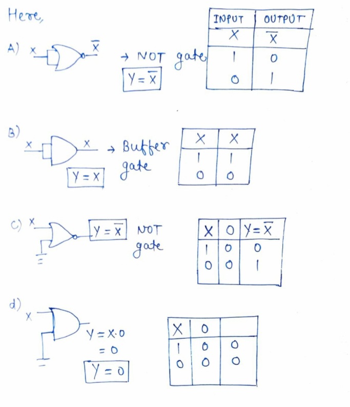
2) What do the circuits shown below do? Expression your answers both as truth tables and as algebraic expressions. D
2) What do the circuits shown below do? Expression your answers both as truth tables and as algebraic expressions. D
Related questions
Question

Transcribed Image Text:The image contains a question with diagrams of logic circuits labeled A, B, C, and D. The task is to determine the function of each circuit and express the answers as both truth tables and algebraic expressions.
**Detail of Each Circuit Diagram:**
- **Diagram A:**
- Contains a logic gate with three inputs.
- One input is directly connected to the gate, while two are connected in series, suggesting an AND gate.
- The AND gate appears to have an inversion bubble on the output, indicating a NAND gate.
- **Diagram B:**
- Contains a similar structure to Diagram A but with three inputs.
- The inputs suggest another AND gate configuration.
- It also seems to have an inversion bubble on the output, indicating a NAND gate.
- **Diagram C:**
- Displays a logic gate with one connection leading to ground, indicating one input is permanently set to 0.
- This, combined with the other input, suggests the gate could be functioning as a NOT gate.
- The presence of an inversion bubble is likely indicating another logic gate operation.
- **Diagram D:**
- Similar to Diagram C, with one input connected to the ground.
- Appears to also feature an inversion bubble on the output.
**Guidance for Creating Truth Tables and Algebraic Expressions:**
1. **Determine the Type of Each Logic Gate:**
- Identify the basic operation of the gate (AND, OR, NOT, NAND, NOR, etc.).
2. **Recognize the Inputs and Outputs:**
- Analyze the number and configuration of inputs.
3. **Create Truth Tables:**
- List all possible input combinations and their corresponding outputs based on gate operation.
4. **Algebraic Expressions:**
- Use Boolean algebra to express the gate functions (e.g., `A ⋅ B`, `A + B`, `¬A`).
The task is to analyze each circuit and then translate its operation into Boolean expressions and truth tables.
Expert Solution
Step 1

Step by step
Solved in 2 steps with 1 images
